
ADC0801/ADC0802/ADC0803/ADC0804/ADC0805
8-Bit µP Compatible A/D Converters
General Description
The
ADC0801,
ADC0802,
ADC0803,
ADC0804
and
ADC0805 are CMOS 8-bit successive approximation A/D
converters
that
use
a
differential
potentiometric
ladder -- similar to the 256R products. These converters are
designed to allow operation with the NSC800 and INS8080A
derivative control bus with TRI-STATE
Æ
output latches di-
rectly driving the data bus. These A/Ds appear like memory
locations or I/O ports to the microprocessor and no interfac-
ing logic is needed.
Differential analog voltage inputs allow increasing the
common-mode rejection and offsetting the analog zero input
voltage value. In addition, the voltage reference input can be
adjusted to allow encoding any smaller analog voltage span
to the full 8 bits of resolution.
Features
n
Compatible with 8080 µP derivatives -- no interfacing
logic needed - access time - 135 ns
n
Easy interface to all microprocessors, or operates "stand
alone"
n
Differential analog voltage inputs
n
Logic inputs and outputs meet both MOS and TTL
voltage level specifications
n
Works with 2.5V (LM336) voltage reference
n
On-chip clock generator
n
0V to 5V analog input voltage range with single 5V
supply
n
No zero adjust required
n
0.3" standard width 20-pin DIP package
n
20-pin molded chip carrier or small outline package
n
Operates ratiometrically or with 5 V
DC
, 2.5 V
DC
, or
analog span adjusted voltage reference
Key Specifications
n
Resolution
8 bits
n
Total error
±
1
/
4
LSB,
±
1
/
2
LSB and
±
1 LSB
n
Conversion time
100 µs
Connection Diagram
Ordering Information
TEMP RANGE
0∞C TO 70∞C
0∞C TO 70∞C
-40∞C TO +85∞C
±
1
/
4
Bit Adjusted
ADC0801LCN
ERROR
±
1
/
2
Bit Unadjusted
ADC0802LCWM
ADC0802LCN
±
1
/
2
Bit Adjusted
ADC0803LCN
±
1Bit Unadjusted
ADC0804LCWM
ADC0804LCN
ADC0805LCN/ADC0804LCJ
PACKAGE OUTLINE
M20B -- Small
Outline
N20A -- Molded DIP
TRI-STATE
Æ
is a registered trademark of National Semiconductor Corp.
Z-80
Æ
is a registered trademark of Zilog Corp.
ADC080X
Dual-In-Line and Small Outline (SO) Packages
DS005671-30
See Ordering Information
November 1999
ADC0801/ADC0802/ADC0803/ADC0804/ADC0805
8-Bit
µP
Compatible
A/D
Converters
© 1999 National Semiconductor Corporation
DS005671
www.national.com

Typical Applications
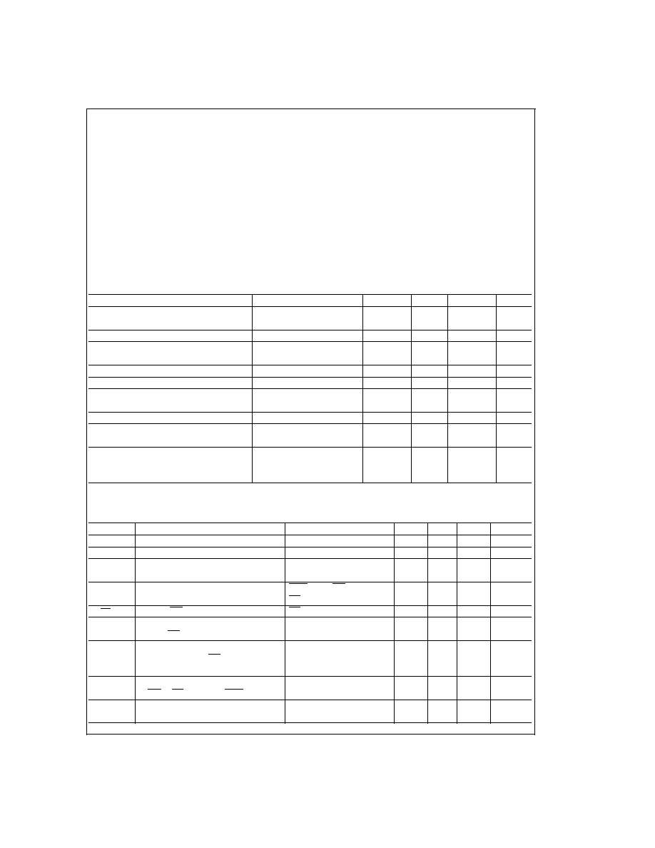
Error Specification (Includes Full-Scale,
Zero Error, and Non-Linearity)
Part
Full-
V
REF
/2=2.500 V
DC
V
REF
/2=No Connection
Number
Scale
(No Adjustments)
(No Adjustments)
Adjusted
ADC0801
±
1
/
4
LSB
ADC0802
±
1
/
2
LSB
ADC0803
±
1
/
2
LSB
ADC0804
±
1 LSB
ADC0805
±
1 LSB
DS005671-1
8080 Interface
DS005671-31
ADC0801/ADC0802/ADC0803/ADC0804/ADC0805
www.national.com
2
Absolute Maximum Ratings
(Notes 1, 2)
If Military/Aerospace specified devices are required,
please contact the National Semiconductor Sales Office/
Distributors for availability and specifications.
Supply Voltage (V
CC
) (Note 3)
6.5V
Voltage
Logic Control Inputs
-0.3V to +18V
At Other Input and Outputs
-0.3V to (V
CC
+0.3V)
Lead Temp. (Soldering, 10 seconds)
Dual-In-Line Package (plastic)
260∞C
Dual-In-Line Package (ceramic)
300∞C
Surface Mount Package
Vapor Phase (60 seconds)
215∞C
Infrared (15 seconds)
220∞C
Storage Temperature Range
-65∞C to +150∞C
Package Dissipation at T
A
=25∞C
875 mW
ESD Susceptibility (Note 10)
800V
Operating Ratings
(Notes 1, 2)
Temperature Range
T
MIN
T
A
T
MAX
ADC0804LCJ
-40∞C
T
A
+85∞C
ADC0801/02/03/05LCN
-40∞C
T
A
+85∞C
ADC0804LCN
0∞C
T
A
+70∞C
ADC0802/04LCWM
0∞C
T
A
+70∞C
Range of V
CC
4.5 V
DC
to 6.3 V
DC
Electrical Characteristics
The following specifications apply for V
CC
=5 V
DC
, T
MIN
T
A
T
MAX
and f
CLK
=640 kHz unless otherwise specified.
Parameter
Conditions
Min
Typ
Max
Units
ADC0801: Total Adjusted Error (Note 8)
With Full-Scale Adj.
±
1
/
4
LSB
(See Section 2.5.2)
ADC0802: Total Unadjusted Error (Note 8)
V
REF
/2=2.500 V
DC
±
1
/
2
LSB
ADC0803: Total Adjusted Error (Note 8)
With Full-Scale Adj.
±
1
/
2
LSB
(See Section 2.5.2)
ADC0804: Total Unadjusted Error (Note 8)
V
REF
/2=2.500 V
DC
±
1
LSB
ADC0805: Total Unadjusted Error (Note 8)
V
REF
/2-No Connection
±
1
LSB
V
REF
/2 Input Resistance (Pin 9)
ADC0801/02/03/05
2.5
8.0
k
ADC0804 (Note 9)
0.75
1.1
k
Analog Input Voltage Range
(Note 4) V(+) or V(-)
Gnd≠0.05
V
CC
+0.05
V
DC
DC Common-Mode Error
Over Analog Input Voltage
±
1/16
±
1
/
8
LSB
Range
Power Supply Sensitivity
V
CC
=5 V
DC
±
10% Over
±
1/16
±
1
/
8
LSB
Allowed V
IN
(+) and V
IN
(-)
Voltage Range (Note 4)
AC Electrical Characteristics
The following specifications apply for V
CC
=5 V
DC
and T
MIN
T
A
T
MAX
unless otherwise specified.
Symbol
Parameter
Conditions
Min
Typ
Max
Units
T
C
Conversion Time
f
CLK
=640 kHz (Note 6)
103
114
µs
T
C
Conversion Time
(Notes 5, 6)
66
73
1/f
CLK
f
CLK
Clock Frequency
V
CC
=5V, (Note 5)
100
640
1460
kHz
Clock Duty Cycle
40
60
%
CR
Conversion Rate in Free-Running
INTR tied to WR with
8770
9708
conv/s
Mode
CS =0 V
DC
, f
CLK
=640 kHz
t
W(WR)L
Width of WR Input (Start Pulse Width)
CS =0 V
DC
(Note 7)
100
ns
t
ACC
Access Time (Delay from Falling
C
L
=100 pF
135
200
ns
Edge of RD to Output Data Valid)
t
1H
, t
0H
TRI-STATE Control (Delay
C
L
=10 pF, R
L
=10k
125
200
ns
from Rising Edge of RD to
(See TRI-STATE Test
Hi-Z State)
Circuits)
t
WI
, t
RI
Delay from Falling Edge
300
450
ns
of WR or RD to Reset of INTR
C
IN
Input Capacitance of Logic
5
7.5
pF
Control Inputs
ADC0801/ADC0802/ADC0803/ADC0804/ADC0805
www.national.com
3

AC Electrical Characteristics
(Continued)
The following specifications apply for V
CC
=5 V
DC
and T
MIN
T
A
T
MAX
unless otherwise specified.
Symbol
Parameter
Conditions
Min
Typ
Max
Units
C
OUT
TRI-STATE Output
5
7.5
pF
Capacitance (Data Buffers)
CONTROL INPUTS [Note: CLK IN (Pin 4) is the input of a Schmitt trigger circuit and is therefore specified separately]
V
IN
(1)
Logical "1" Input Voltage
V
CC
=5.25 V
DC
2.0
15
V
DC
(Except Pin 4 CLK IN)
V
IN
(0)
Logical "0" Input Voltage
V
CC
=4.75 V
DC
0.8
V
DC
(Except Pin 4 CLK IN)
I
IN
(1)
Logical "1" Input Current
V
IN
=5 V
DC
0.005
1
µA
DC
(All Inputs)
I
IN
(0)
Logical "0" Input Current
V
IN
=0 V
DC
-1
-0.005
µA
DC
(All Inputs)
CLOCK IN AND CLOCK R
V
T
+
CLK IN (Pin 4) Positive Going
2.7
3.1
3.5
V
DC
Threshold Voltage
V
T
-
CLK IN (Pin 4) Negative
1.5
1.8
2.1
V
DC
Going Threshold Voltage
V
H
CLK IN (Pin 4) Hysteresis
0.6
1.3
2.0
V
DC
(V
T
+)-(V
T
-)
V
OUT
(0)
Logical "0" CLK R Output
I
O
=360 µA
0.4
V
DC
Voltage
V
CC
=4.75 V
DC
V
OUT
(1)
Logical "1" CLK R Output
I
O
=-360 µA
2.4
V
DC
Voltage
V
CC
=4.75 V
DC
DATA OUTPUTS AND INTR
V
OUT
(0)
Logical "0" Output Voltage
Data Outputs
I
OUT
=1.6 mA, V
CC
=4.75 V
DC
0.4
V
DC
INTR Output
I
OUT
=1.0 mA, V
CC
=4.75 V
DC
0.4
V
DC
V
OUT
(1)
Logical "1" Output Voltage
I
O
=-360 µA, V
CC
=4.75 V
DC
2.4
V
DC
V
OUT
(1)
Logical "1" Output Voltage
I
O
=-10 µA, V
CC
=4.75 V
DC
4.5
V
DC
I
OUT
TRI-STATE Disabled Output
V
OUT
=0 V
DC
-3
µA
DC
Leakage (All Data Buffers)
V
OUT
=5 V
DC
3
µA
DC
I
SOURCE
V
OUT
Short to Gnd, T
A
=25∞C
4.5
6
mA
DC
I
SINK
V
OUT
Short to V
CC
, T
A
=25∞C
9.0
16
mA
DC
POWER SUPPLY
I
CC
Supply Current (Includes
f
CLK
=640 kHz,
Ladder Current)
V
REF
/2=NC, T
A
=25∞C
and CS =5V
ADC0801/02/03/04LCJ/05
1.1
1.8
mA
ADC0804LCN/LCWM
1.9
2.5
mA
Note 1: Absolute Maximum Ratings indicate limits beyond which damage to the device may occur. DC and AC electrical specifications do not apply when operating
the device beyond its specified operating conditions.
Note 2: All voltages are measured with respect to Gnd, unless otherwise specified. The separate A Gnd point should always be wired to the D Gnd.
Note 3: A zener diode exists, internally, from V
CC
to Gnd and has a typical breakdown voltage of 7 V
DC
.
Note 4: For V
IN
(-)
V
IN
(+) the digital output code will be 0000 0000. Two on-chip diodes are tied to each analog input (see block diagram) which will forward conduct
for analog input voltages one diode drop below ground or one diode drop greater than the V
CC
supply. Be careful, during testing at low V
CC
levels (4.5V), as high
level analog inputs (5V) can cause this input diode to conduct≠especially at elevated temperatures, and cause errors for analog inputs near full-scale. The spec allows
50 mV forward bias of either diode. This means that as long as the analog V
IN
does not exceed the supply voltage by more than 50 mV, the output code will be correct.
To achieve an absolute 0 V
DC
to 5 V
DC
input voltage range will therefore require a minimum supply voltage of 4.950 V
DC
over temperature variations, initial tolerance
and loading.
Note 5: Accuracy is guaranteed at f
CLK
= 640 kHz. At higher clock frequencies accuracy can degrade. For lower clock frequencies, the duty cycle limits can be ex-
tended so long as the minimum clock high time interval or minimum clock low time interval is no less than 275 ns.
Note 6: With an asynchronous start pulse, up to 8 clock periods may be required before the internal clock phases are proper to start the conversion process. The
start request is internally latched, see
Figure 4 and section 2.0.
ADC0801/ADC0802/ADC0803/ADC0804/ADC0805
www.national.com
4

AC Electrical Characteristics
(Continued)
Note 7: The CS input is assumed to bracket the WR strobe input and therefore timing is dependent on the WR pulse width. An arbitrarily wide pulse width will hold
the converter in a reset mode and the start of conversion is initiated by the low to high transition of the WR pulse (see timing diagrams).
Note 8: None of these A/Ds requires a zero adjust (see section 2.5.1). To obtain zero code at other analog input voltages see section 2.5 and
Figure 7.
Note 9: The V
REF
/2 pin is the center point of a two-resistor divider connected from V
CC
to ground. In all versions of the ADC0801, ADC0802, ADC0803, and
ADC0805, and in the ADC0804LCJ, each resistor is typically 16 k
. In all versions of the ADC0804 except the ADC0804LCJ, each resistor is typically 2.2 k
.
Note 10: Human body model, 100 pF discharged through a 1.5 k
resistor.
Typical Performance Characteristics
Logic Input Threshold Voltage
vs. Supply Voltage
DS005671-38
Delay From Falling Edge of
RD to Output Data Valid
vs. Load Capacitance
DS005671-39
CLK IN Schmitt Trip Levels
vs. Supply Voltage
DS005671-40
f
CLK
vs. Clock Capacitor
DS005671-41
Full-Scale Error vs
Conversion Time
DS005671-42
Effect of Unadjusted Offset Error
vs. V
REF
/2 Voltage
DS005671-43
Output Current vs
Temperature
DS005671-44
Power Supply Current
vs Temperature (Note 9)
DS005671-45
Linearity Error at Low
V
REF
/2 Voltages
DS005671-46
ADC0801/ADC0802/ADC0803/ADC0804/ADC0805
www.national.com
5