 | –≠–ª–µ–∫—Ç—Ä–æ–Ω–Ω—ã–π –∫–æ–º–ø–æ–Ω–µ–Ω—Ç: ADC0808CJ | –°–∫–∞—á–∞—Ç—å:  PDF PDF  ZIP ZIP |
ADC0808/ADC0809
8-Bit µP Compatible A/D Converters with 8-Channel
Multiplexer
General Description
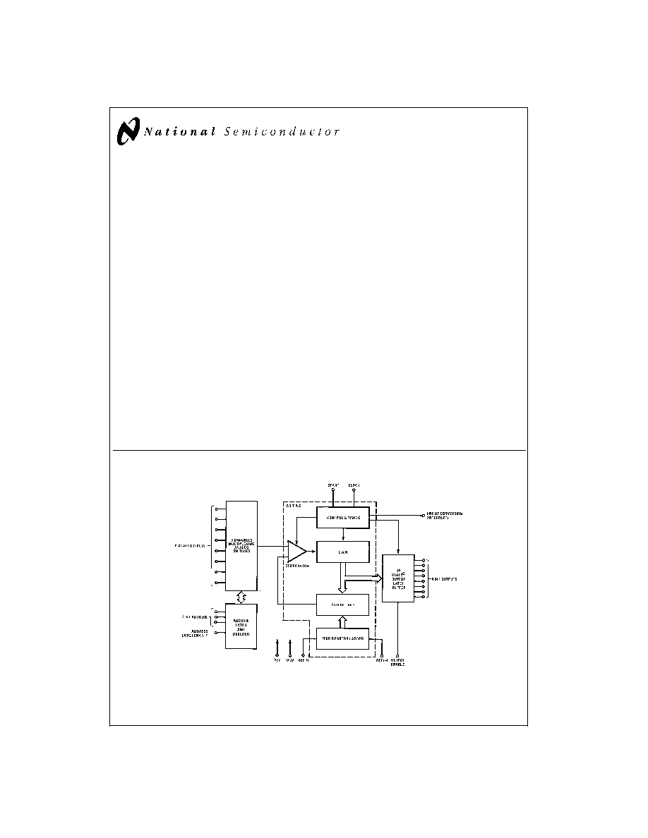
The ADC0808, ADC0809 data acquisition component is a
monolithic CMOS device with an 8-bit analog-to-digital con-
verter, 8-channel multiplexer and microprocessor compatible
control logic. The 8-bit A/D converter uses successive ap-
proximation as the conversion technique. The converter fea-
tures a high impedance chopper stabilized comparator, a
256R voltage divider with analog switch tree and a succes-
sive approximation register. The 8-channel multiplexer can
directly access any of 8-single-ended analog signals.
The device eliminates the need for external zero and
full-scale adjustments. Easy interfacing to microprocessors
is provided by the latched and decoded multiplexer address
inputs and latched TTL TRI-STATE
Æ
outputs.
The design of the ADC0808, ADC0809 has been optimized
by incorporating the most desirable aspects of several A/D
conversion techniques. The ADC0808, ADC0809 offers high
speed, high accuracy, minimal temperature dependence, ex-
cellent long-term accuracy and repeatability, and consumes
minimal power. These features make this device ideally
suited to applications from process and machine control to
consumer and automotive applications. For 16-channel mul-
tiplexer
with
common
output
(sample/hold
port)
see
ADC0816 data sheet. (See AN-247 for more information.)
Features
n
Easy interface to all microprocessors
n
Operates ratiometrically or with 5 V
DC
or analog span
adjusted voltage reference
n
No zero or full-scale adjust required
n
8-channel multiplexer with address logic
n
0V to 5V input range with single 5V power supply
n
Outputs meet TTL voltage level specifications
n
Standard hermetic or molded 28-pin DIP package
n
28-pin molded chip carrier package
n
ADC0808 equivalent to MM74C949
n
ADC0809 equivalent to MM74C949-1
Key Specifications
n
Resolution
8 Bits
n
Total Unadjusted Error
±
1
/
2
LSB and
±
1 LSB
n
Single Supply
5 V
DC
n
Low Power
15 mW
n
Conversion Time
100 µs
Block Diagram
TRI-STATE
Æ
is a registered trademark of National Semiconductor Corp.
DS005672-1
See Ordering
Information
October 1999
ADC0808/ADC0809
8-Bit
µP
Compatible
A/D
Converters
with
8-Channel
Multiplexer
© 1999 National Semiconductor Corporation
DS005672
www.national.com
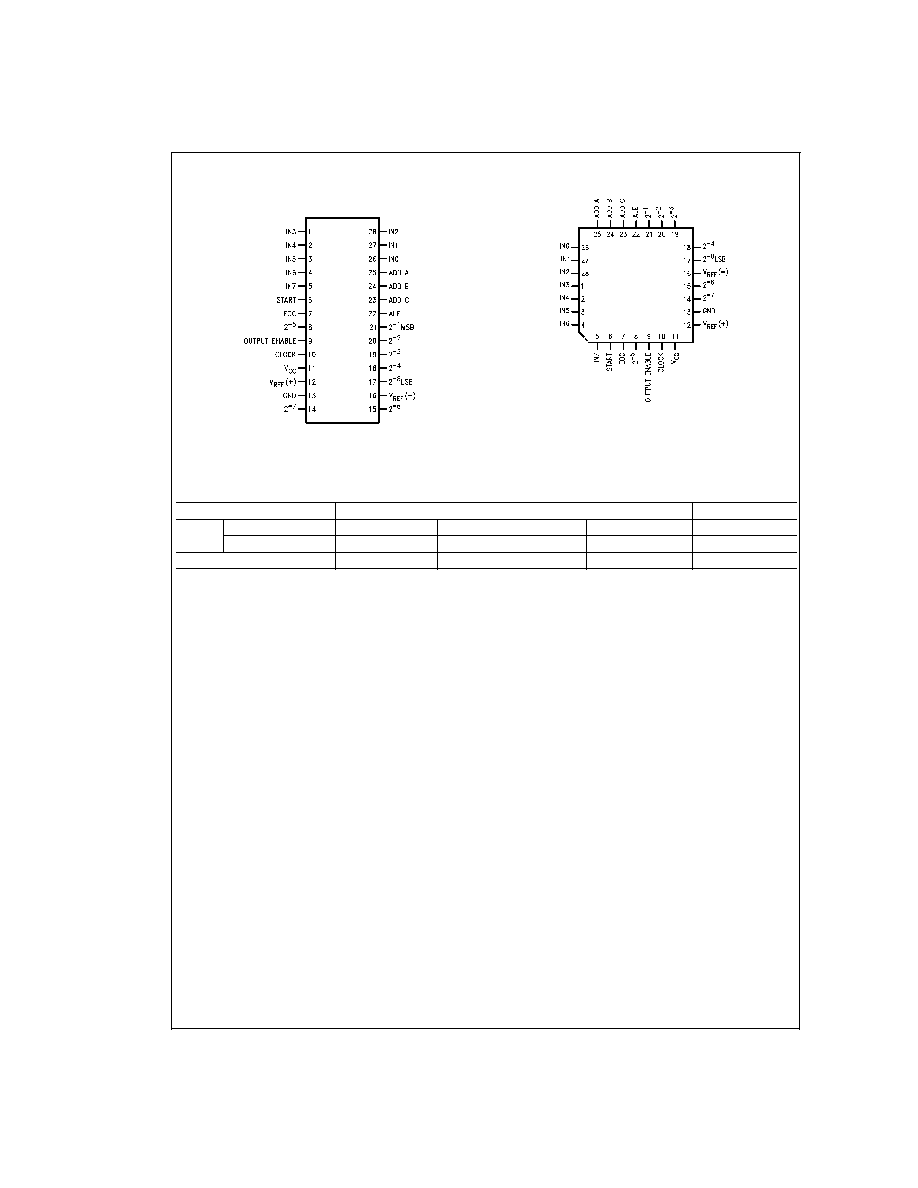
Connection Diagrams
Ordering Information
TEMPERATURE RANGE
-40∞C to +85∞C
-55∞C to +125∞C
Error
±
1
/
2
LSB Unadjusted
ADC0808CCN
ADC0808CCV
ADC0808CCJ
ADC0808CJ
±
1 LSB Unadjusted
ADC0809CCN
ADC0809CCV
Package Outline
N28A Molded DIP
V28A Molded Chip Carrier
J28A Ceramic DIP
J28A Ceramic DIP
Dual-In-Line Package
DS005672-11
Order Number ADC0808CCN or ADC0809CCN
See NS Package J28A or N28A
Molded Chip Carrier Package
DS005672-12
Order Number ADC0808CCV or ADC0809CCV
See NS Package V28A
ADC0808/ADC0809
www.national.com
2

Absolute Maximum Ratings
(Notes 2, 1)
If Military/Aerospace specified devices are required,
please contact the National Semiconductor Sales Office/
Distributors for availability and specifications.
Supply Voltage (V
CC
) (Note 3)
6.5V
Voltage at Any Pin
-0.3V to (V
CC
+0.3V)
Except Control Inputs
Voltage at Control Inputs
-0.3V to +15V
(START, OE, CLOCK, ALE, ADD A, ADD B, ADD C)
Storage Temperature Range
-65∞C to +150∞C
Package Dissipation at T
A
=25∞C
875 mW
Lead Temp. (Soldering, 10 seconds)
Dual-In-Line Package (plastic)
260∞C
Dual-In-Line Package (ceramic)
300∞C
Molded Chip Carrier Package
Vapor Phase (60 seconds)
215∞C
Infrared (15 seconds)
220∞C
ESD Susceptibility (Note 8)
400V
Operating Conditions
(Notes 1, 2)
Temperature Range (Note 1)
T
MIN
T
A
T
MAX
ADC0808CCN,ADC0809CCN
-40∞C
T
A
+85∞C
ADC0808CCV, ADC0809CCV
-40∞C
T
A
+85∞C
Range of V
CC
(Note 1)
4.5 V
DC
to 6.0 V
DC
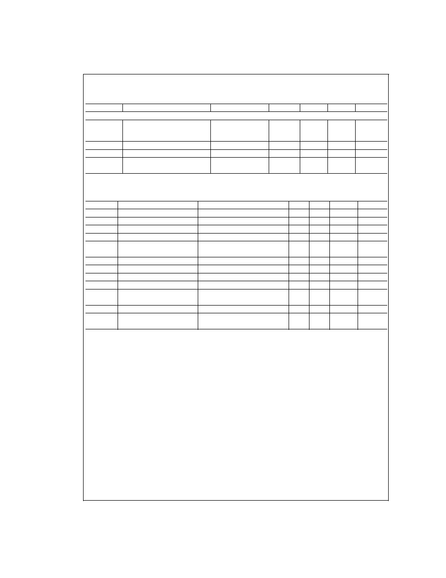
Electrical Characteristics
Converter Specifications: V
CC
=5 V
DC
=V
REF+
, V
REF(-)
=GND, T
MIN
T
A
T
MAX
and f
CLK
=640 kHz unless otherwise stated.
Symbol
Parameter
Conditions
Min
Typ
Max
Units
ADC0808
Total Unadjusted Error
25∞C
±
1
/
2
LSB
(Note 5)
T
MIN
to T
MAX
±
3
/
4
LSB
ADC0809
Total Unadjusted Error
0∞C to 70∞C
±
1
LSB
(Note 5)
T
MIN
to T
MAX
±
1
1
/
4
LSB
Input Resistance
From Ref(+) to Ref(-)
1.0
2.5
k
Analog Input Voltage Range
(Note 4) V(+) or V(-)
GND-0.10
V
CC
+0.10
V
DC
V
REF(+)
Voltage, Top of Ladder
Measured at Ref(+)
V
CC
V
CC
+0.1
V
Voltage, Center of Ladder
V
CC
/2-0.1
V
CC
/2
V
CC
/2+0.1
V
V
REF(-)
Voltage, Bottom of Ladder
Measured at Ref(-)
-0.1
0
V
I
IN
Comparator Input Current
f
c
=640 kHz, (Note 6)
-2
±
0.5
2
µA
Electrical Characteristics
Digital Levels and DC Specifications: ADC0808CCN, ADC0808CCV, ADC0809CCN and ADC0809CCV, 4.75
V
CC
5.25V,
-40∞C
T
A
+85∞C unless otherwise noted
Symbol
Parameter
Conditions
Min
Typ
Max
Units
ANALOG MULTIPLEXER
I
OFF(+)
OFF Channel Leakage Current
V
CC
=5V, V
IN
=5V,
T
A
=25∞C
10
200
nA
T
MIN
to T
MAX
1.0
µA
I
OFF(-)
OFF Channel Leakage Current
V
CC
=5V, V
IN
=0,
T
A
=25∞C
-200
-10
nA
T
MIN
to T
MAX
-1.0
µA
CONTROL INPUTS
V
IN(1)
Logical "1" Input Voltage
V
CC
-1.5
V
V
IN(0)
Logical "0" Input Voltage
1.5
V
I
IN(1)
Logical "1" Input Current
V
IN
=15V
1.0
µA
(The Control Inputs)
I
IN(0)
Logical "0" Input Current
V
IN
=0
-1.0
µA
(The Control Inputs)
I
CC
Supply Current
f
CLK
=640 kHz
0.3
3.0
mA
ADC0808/ADC0809
www.national.com
3
Electrical Characteristics
(Continued)
Digital Levels and DC Specifications: ADC0808CCN, ADC0808CCV, ADC0809CCN and ADC0809CCV, 4.75
V
CC
5.25V,
-40∞C
T
A
+85∞C unless otherwise noted
Symbol
Parameter
Conditions
Min
Typ
Max
Units
DATA OUTPUTS AND EOC (INTERRUPT)
V
OUT(1)
Logical "1" Output Voltage
V
CC
= 4.75V
I
OUT
= -360µA
I
OUT
= -10µA
2.4
4.5
V(min)
V(min)
V
OUT(0)
Logical "0" Output Voltage
I
O
=1.6 mA
0.45
V
V
OUT(0)
Logical "0" Output Voltage EOC
I
O
=1.2 mA
0.45
V
I
OUT
TRI-STATE Output Current
V
O
=5V
3
µA
V
O
=0
-3
µA
Electrical Characteristics
Timing Specifications V
CC
=V
REF(+)
=5V, V
REF(-)
=GND, t
r
=t
f
=20 ns and T
A
=25∞C unless otherwise noted.
Symbol
Parameter
Conditions
MIn
Typ
Max
Units
t
WS
Minimum Start Pulse Width
(
Figure 5)
100
200
ns
t
WALE
Minimum ALE Pulse Width
(
Figure 5)
100
200
ns
t
s
Minimum Address Set-Up Time
(
Figure 5)
25
50
ns
t
H
Minimum Address Hold Time
(
Figure 5)
25
50
ns
t
D
Analog MUX Delay Time
R
S
=0
(
Figure 5)
1
2.5
µs
From ALE
t
H1
, t
H0
OE Control to Q Logic State
C
L
=50 pF, R
L
=10k (Figure 8)
125
250
ns
t
1H
, t
0H
OE Control to Hi-Z
C
L
=10 pF, R
L
=10k (Figure 8)
125
250
ns
t
c
Conversion Time
f
c
=640 kHz, (Figure 5) (Note 7)
90
100
116
µs
f
c
Clock Frequency
10
640
1280
kHz
t
EOC
EOC Delay Time
(
Figure 5)
0
8+2 µS
Clock
Periods
C
IN
Input Capacitance
At Control Inputs
10
15
pF
C
OUT
TRI-STATE Output
At TRI-STATE Outputs
10
15
pF
Capacitance
Note 1: Absolute Maximum Ratings indicate limits beyond which damage to the device may occur. DC and AC electrical specifications do not apply when operating
the device beyond its specified operating conditions.
Note 2: All voltages are measured with respect to GND, unless othewise specified.
Note 3: A zener diode exists, internally, from V
CC
to GND and has a typical breakdown voltage of 7 V
DC
.
Note 4: Two on-chip diodes are tied to each analog input which will forward conduct for analog input voltages one diode drop below ground or one diode drop greater
than the V
CC
n supply. The spec allows 100 mV forward bias of either diode. This means that as long as the analog V
IN
does not exceed the supply voltage by more
than 100 mV, the output code will be correct. To achieve an absolute 0V
DC
to 5V
DC
input voltage range will therefore require a minimum supply voltage of 4.900 V
DC
over temperature variations, initial tolerance and loading.
Note 5: Total unadjusted error includes offset, full-scale, linearity, and multiplexer errors. See
Figure 3. None of these A/Ds requires a zero or full-scale adjust. How-
ever, if an all zero code is desired for an analog input other than 0.0V, or if a narrow full-scale span exists (for example: 0.5V to 4.5V full-scale) the reference voltages
can be adjusted to achieve this. See
Figure 13.
Note 6: Comparator input current is a bias current into or out of the chopper stabilized comparator. The bias current varies directly with clock frequency and has little
temperature dependence (
Figure 6). See paragraph 4.0.
Note 7: The outputs of the data register are updated one clock cycle before the rising edge of EOC.
Note 8: Human body model, 100 pF discharged through a 1.5 k
resistor.
ADC0808/ADC0809
www.national.com
4

Functional Description
Multiplexer. The device contains an 8-channel single-ended
analog signal multiplexer. A particular input channel is se-
lected by using the address decoder.
Table 1 shows the input
states for the address lines to select any channel. The ad-
dress is latched into the decoder on the low-to-high transition
of the address latch enable signal.
TABLE 1.
SELECTED
ADDRESS LINE
ANALOG
CHANNEL
C
B
A
IN0
L
L
L
IN1
L
L
H
IN2
L
H
L
IN3
L
H
H
IN4
H
L
L
IN5
H
L
H
IN6
H
H
L
IN7
H
H
H
CONVERTER CHARACTERISTICS
The Converter
The heart of this single chip data acquisition system is its
8-bit analog-to-digital converter. The converter is designed to
give fast, accurate, and repeatable conversions over a wide
range of temperatures. The converter is partitioned into 3
major sections: the 256R ladder network, the successive ap-
proximation register, and the comparator. The converter's
digital outputs are positive true.
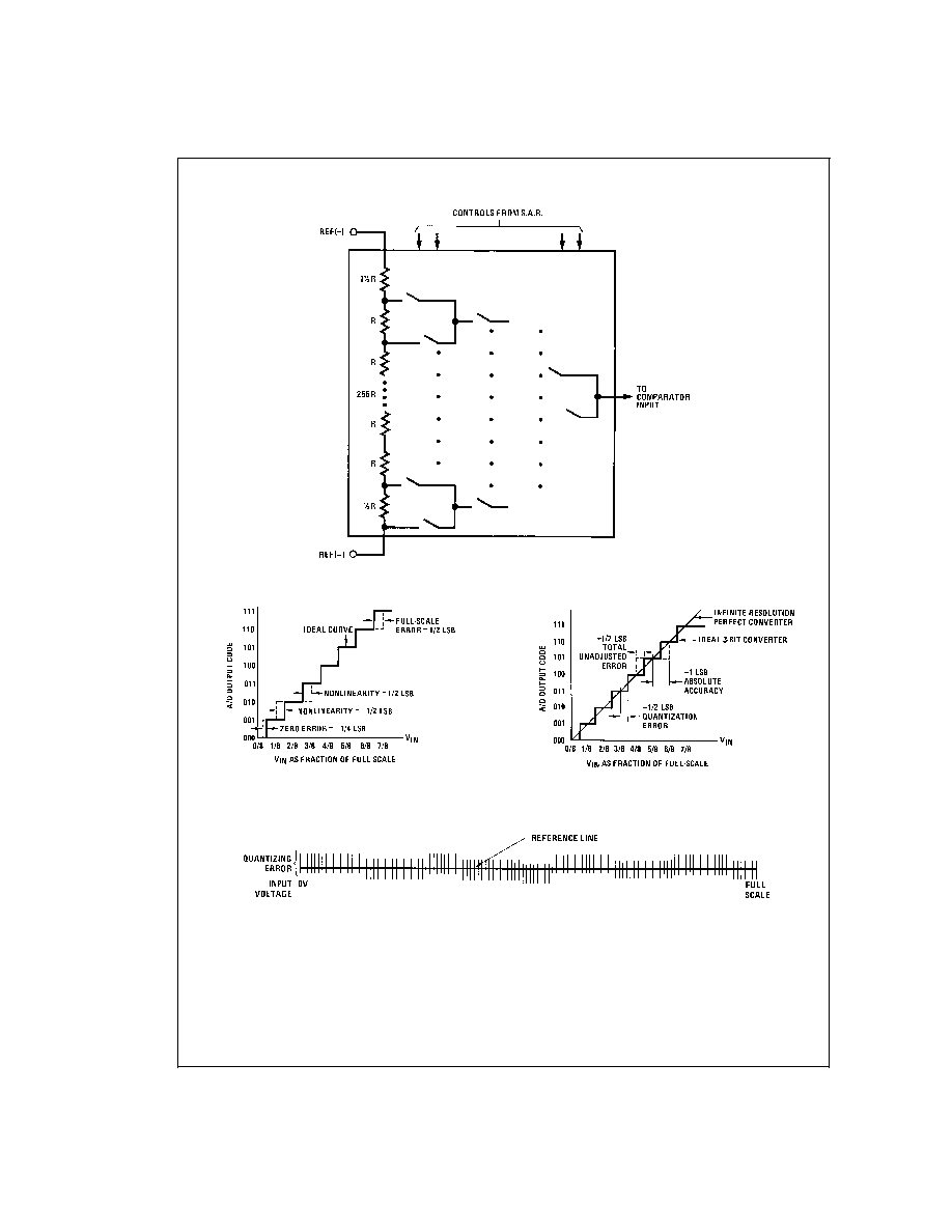
The 256R ladder network approach (
Figure 1) was chosen
over the conventional R/2R ladder because of its inherent
monotonicity, which guarantees no missing digital codes.
Monotonicity is particularly important in closed loop feedback
control systems. A non-monotonic relationship can cause os-
cillations that will be catastrophic for the system. Additionally,
the 256R network does not cause load variations on the ref-
erence voltage.
The bottom resistor and the top resistor of the ladder net-
work in
Figure 1 are not the same value as the remainder of
the network. The difference in these resistors causes the
output characteristic to be symmetrical with the zero and
full-scale points of the transfer curve. The first output transi-
tion occurs when the analog signal has reached +
1
/
2
LSB
and succeeding output transitions occur every 1 LSB later up
to full-scale.
The successive approximation register (SAR) performs 8 it-
erations to approximate the input voltage. For any SAR type
converter, n-iterations are required for an n-bit converter.
Figure 2 shows a typical example of a 3-bit converter. In the
ADC0808, ADC0809, the approximation technique is ex-
tended to 8 bits using the 256R network.
The A/D converter's successive approximation register
(SAR) is reset on the positive edge of the start conversion
(SC) pulse. The conversion is begun on the falling edge of
the start conversion pulse. A conversion in process will be in-
terrupted by receipt of a new start conversion pulse. Con-
tinuous conversion may be accomplished by tying the
end-of-conversion (EOC) output to the SC input. If used in
this mode, an external start conversion pulse should be ap-
plied after power up. End-of-conversion will go low between
0 and 8 clock pulses after the rising edge of start conversion.
The most important section of the A/D converter is the com-
parator. It is this section which is responsible for the ultimate
accuracy of the entire converter. It is also the comparator
drift which has the greatest influence on the repeatability of
the device. A chopper-stabilized comparator provides the
most effective method of satisfying all the converter require-
ments.
The chopper-stabilized comparator converts the DC input
signal into an AC signal. This signal is then fed through a
high gain AC amplifier and has the DC level restored. This
technique limits the drift component of the amplifier since the
drift is a DC component which is not passed by the AC am-
plifier. This makes the entire A/D converter extremely insen-
sitive to temperature, long term drift and input offset errors.
Figure 4 shows a typical error curve for the ADC0808 as
measured using the procedures outlined in AN-179.
ADC0808/ADC0809
www.national.com
5
Functional Description
(Continued)
DS005672-2
FIGURE 1. Resistor Ladder and Switch Tree
DS005672-13
FIGURE 2. 3-Bit A/D Transfer Curve
DS005672-14
FIGURE 3. 3-Bit A/D Absolute Accuracy Curve
DS005672-15
FIGURE 4. Typical Error Curve
ADC0808/ADC0809
www.national.com
6
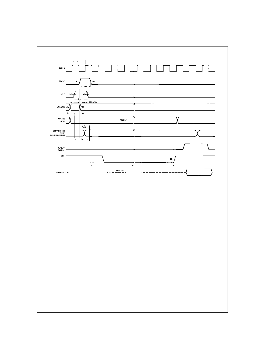
Timing Diagram
DS005672-4
FIGURE 5.
ADC0808/ADC0809
www.national.com
7

Typical Performance Characteristics
TRI-STATE Test Circuits and Timing Diagrams
Applications Information
OPERATION
1.0 RATIOMETRIC CONVERSION
The ADC0808, ADC0809 is designed as a complete Data
Acquisition System (DAS) for ratiometric conversion sys-
tems. In ratiometric systems, the physical variable being
measured is expressed as a percentage of full-scale which is
not necessarily related to an absolute standard. The voltage
input to the ADC0808 is expressed by the equation
(1)
V
IN
=Input voltage into the ADC0808
V
fs
=Full-scale voltage
V
Z
=Zero voltage
D
X
=Data point being measured
D
MAX
=Maximum data limit
D
MIN
=Minimum data limit
A good example of a ratiometric transducer is a potentiom-
eter used as a position sensor. The position of the wiper is di-
rectly proportional to the output voltage which is a ratio of the
full-scale voltage across it. Since the data is represented as
a proportion of full-scale, reference requirements are greatly
reduced, eliminating a large source of error and cost for
many applications. A major advantage of the ADC0808,
ADC0809 is that the input voltage range is equal to the sup-
ply range so the transducers can be connected directly
across the supply and their outputs connected directly into
the multiplexer inputs, (
Figure 9).
Ratiometric transducers such as potentiometers, strain
gauges, thermistor bridges, pressure transducers, etc., are
suitable for measuring proportional relationships; however,
many types of measurements must be referred to an abso-
lute standard such as voltage or current. This means a sys-
DS005672-16
FIGURE 6. Comparator I
IN
vs V
IN
(V
CC
=V
REF
=5V)
DS005672-17
FIGURE 7. Multiplexer R
ON
vs V
IN
(V
CC
=V
REF
=5V)
t
1H
, t
H1
DS005672-18
t
1H
, C
L
= 10 pF
DS005672-19
t
H1
, C
L
= 50 pF
DS005672-20
t
0H
, t
H0
DS005672-21
t
0H
, C
L
= 10 pF
DS005672-22
t
H0
, C
L
= 50 pF
DS005672-23
FIGURE 8.
ADC0808/ADC0809
www.national.com
8

Applications Information
(Continued)
tem reference must be used which relates the full-scale volt-
age to the standard volt. For example, if V
CC
=V
REF
=5.12V,
then the full-scale range is divided into 256 standard steps.
The smallest standard step is 1 LSB which is then 20 mV.
2.0 RESISTOR LADDER LIMITATIONS
The voltages from the resistor ladder are compared to the
selected into 8 times in a conversion. These voltages are
coupled to the comparator via an analog switch tree which is
referenced to the supply. The voltages at the top, center and
bottom of the ladder must be controlled to maintain proper
operation.
The top of the ladder, Ref(+), should not be more positive
than the supply, and the bottom of the ladder, Ref(-), should
not be more negative than ground. The center of the ladder
voltage must also be near the center of the supply because
the analog switch tree changes from N-channel switches to
P-channel switches. These limitations are automatically sat-
isfied in ratiometric systems and can be easily met in ground
referenced systems.
Figure 10 shows a ground referenced system with a sepa-
rate supply and reference. In this system, the supply must be
trimmed to match the reference voltage. For instance, if a
5.12V is used, the supply should be adjusted to the same
voltage within 0.1V.
The ADC0808 needs less than a milliamp of supply current
so developing the supply from the reference is readily ac-
complished. In
Figure 11 a ground referenced system is
shown which generates the supply from the reference. The
buffer shown can be an op amp of sufficient drive to supply
the milliamp of supply current and the desired bus drive, or if
a capacitive bus is driven by the outputs a large capacitor will
supply the transient supply current as seen in
Figure 12. The
LM301 is overcompensated to insure stability when loaded
by the 10 µF output capacitor.
The top and bottom ladder voltages cannot exceed V
CC
and
ground, respectively, but they can be symmetrically less than
V
CC
and greater than ground. The center of the ladder volt-
age should always be near the center of the supply. The sen-
sitivity of the converter can be increased, (i.e., size of the
LSB steps decreased) by using a symmetrical reference sys-
tem. In
Figure 13, a 2.5V reference is symmetrically cen-
tered about V
CC
/2 since the same current flows in identical
resistors. This system with a 2.5V reference allows the LSB
bit to be half the size of a 5V reference system.
DS005672-7
FIGURE 9. Ratiometric Conversion System
ADC0808/ADC0809
www.national.com
9

Applications Information
(Continued)
DS005672-24
FIGURE 10. Ground Referenced
Conversion System Using Trimmed Supply
DS005672-25
FIGURE 11. Ground Referenced Conversion System with
Reference Generating V
CC
Supply
ADC0808/ADC0809
www.national.com
10

Applications Information
(Continued)
3.0 CONVERTER EQUATIONS
The transition between adjacent codes N and N+1 is given
by:
(2)
The center of an output code N is given by:
(3)
The output code N for an arbitrary input are the integers
within the range:
(4)
Where: V
IN
=Voltage at comparator input
V
REF(+)
=Voltage at Ref(+)
V
REF(-)
=Voltage at Ref(-)
V
TUE
=Total unadjusted error voltage (typically
V
REF(+)
˜512)
DS005672-26
FIGURE 12. Typical Reference and Supply Circuit
DS005672-27
R
A
=R
B
*
Ratiometric transducers
FIGURE 13. Symmetrically Centered Reference
ADC0808/ADC0809
www.national.com
11

Applications Information
(Continued)
4.0 ANALOG COMPARATOR INPUTS
The dynamic comparator input current is caused by the pe-
riodic switching of on-chip stray capacitances. These are
connected alternately to the output of the resistor ladder/
switch tree network and to the comparator input as part of
the operation of the chopper stabilized comparator.
The average value of the comparator input current varies di-
rectly with clock frequency and with V
IN
as shown in
Figure 6.
If no filter capacitors are used at the analog inputs and the
signal source impedances are low, the comparator input cur-
rent should not introduce converter errors, as the transient
created by the capacitance discharge will die out before the
comparator output is strobed.
If input filter capacitors are desired for noise reduction and
signal conditioning they will tend to average out the dynamic
comparator input current. It will then take on the characteris-
tics of a DC bias current whose effect can be predicted con-
ventionally.
Typical Application
TABLE 2. Microprocessor Interface Table
PROCESSOR
READ
WRITE
INTERRUPT (COMMENT)
8080
MEMR
MEMW
INTR (Thru RST Circuit)
8085
RD
WR
INTR (Thru RST Circuit)
Z-80
RD
WR
INT (Thru RST Circuit, Mode 0)
SC/MP
NRDS
NWDS
SA (Thru Sense A)
6800
VMA
∑
2
∑R/W
VMA
∑
∑R/W
IRQA or IRQB (Thru PIA)
DS005672-10
*Address latches needed for 8085 and SC/MP interfacing the ADC0808 to a microprocessor
ADC0808/ADC0809
www.national.com
12
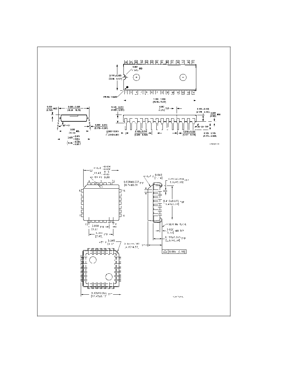
Physical Dimensions
inches (millimeters) unless otherwise noted
Molded Dual-In-Line Package (N)
Order Number ADC0808CCN or ADC0809CCN
NS Package Number N28B
Molded Chip Carrier (V)
Order Number ADC0808CCV or ADC0809CCV
NS Package Number V28A
ADC0808/ADC0809
www.national.com
13

Notes
LIFE SUPPORT POLICY
NATIONAL'S PRODUCTS ARE NOT AUTHORIZED FOR USE AS CRITICAL COMPONENTS IN LIFE SUPPORT
DEVICES OR SYSTEMS WITHOUT THE EXPRESS WRITTEN APPROVAL OF THE PRESIDENT AND GENERAL
COUNSEL OF NATIONAL SEMICONDUCTOR CORPORATION. As used herein:
1. Life support devices or systems are devices or
systems which, (a) are intended for surgical implant
into the body, or (b) support or sustain life, and
whose failure to perform when properly used in
accordance with instructions for use provided in the
labeling, can be reasonably expected to result in a
significant injury to the user.
2. A critical component is any component of a life
support device or system whose failure to perform
can be reasonably expected to cause the failure of
the life support device or system, or to affect its
safety or effectiveness.
National Semiconductor
Corporation
Americas
Tel: 1-800-272-9959
Fax: 1-800-737-7018
Email: support@nsc.com
National Semiconductor
Europe
Fax: +49 (0) 1 80-530 85 86
Email: europe.support@nsc.com
Deutsch Tel: +49 (0) 1 80-530 85 85
English
Tel: +49 (0) 1 80-532 78 32
FranÁais Tel: +49 (0) 1 80-532 93 58
Italiano
Tel: +49 (0) 1 80-534 16 80
National Semiconductor
Asia Pacific Customer
Response Group
Tel: 65-2544466
Fax: 65-2504466
Email: sea.support@nsc.com
National Semiconductor
Japan Ltd.
Tel: 81-3-5639-7560
Fax: 81-3-5639-7507
www.national.com
ADC0808/ADC0809
8-Bit
µP
Compatible
A/D
Converters
with
8-Channel
Multiplexer
National does not assume any responsibility for use of any circuitry described, no circuit patent licenses are implied and National reserves the right at any time without notice to change said circuitry and specifications.