
ADC0808/ADC0809
8-Bit µP Compatible A/D Converters with 8-Channel
Multiplexer
General Description
The ADC0808, ADC0809 data acquisition component is a
monolithic CMOS device with an 8-bit analog-to-digital con-
verter, 8-channel multiplexer and microprocessor compatible
control logic. The 8-bit A/D converter uses successive ap-
proximation as the conversion technique. The converter fea-
tures a high impedance chopper stabilized comparator, a
256R voltage divider with analog switch tree and a succes-
sive approximation register. The 8-channel multiplexer can
directly access any of 8-single-ended analog signals.
The device eliminates the need for external zero and
full-scale adjustments. Easy interfacing to microprocessors
is provided by the latched and decoded multiplexer address
inputs and latched TTL TRI-STATE outputs.
The design of the ADC0808, ADC0809 has been optimized
by incorporating the most desirable aspects of several A/D
conversion techniques. The ADC0808, ADC0809 offers high
speed, high accuracy, minimal temperature dependence,
excellent long-term accuracy and repeatability, and con-
sumes minimal power. These features make this device
ideally suited to applications from process and machine
control to consumer and automotive applications. For
16-channel multiplexer with common output (sample/hold
port) see ADC0816 data sheet. (See AN-247 for more infor-
mation.)
Features
n
Easy interface to all microprocessors
n
Operates ratiometrically or with 5 V
DC
or analog span
adjusted voltage reference
n
No zero or full-scale adjust required
n
8-channel multiplexer with address logic
n
0V to 5V input range with single 5V power supply
n
Outputs meet TTL voltage level specifications
n
ADC0808 equivalent to MM74C949
n
ADC0809 equivalent to MM74C949-1
Key Specifications
n
Resolution
8 Bits
n
Total Unadjusted Error
±
1
/
2
LSB and
±
1 LSB
n
Single Supply
5 V
DC
n
Low Power
15 mW
n
Conversion Time
100 µs
Block Diagram
00567201
See Ordering
Information
October 2002
ADC0808/ADC0809
8-Bit
µP
Compatible
A/D
Converters
with
8-Channel
Multiplexer
© 2002 National Semiconductor Corporation
DS005672
www.national.com
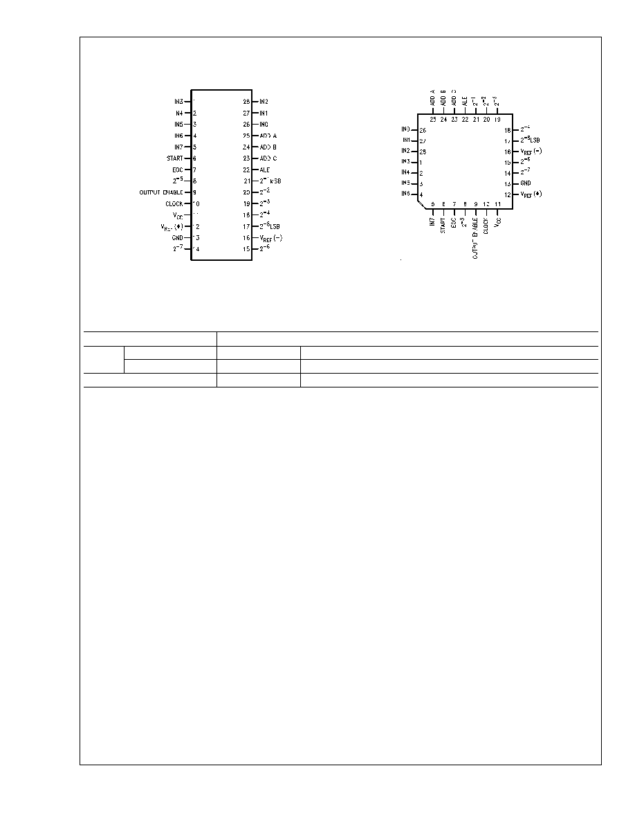
Connection Diagrams
Dual-In-Line Package
00567211
Order Number ADC0808CCN or ADC0809CCN
See NS Package J28A or N28A
Molded Chip Carrier Package
00567212
Order Number ADC0808CCV or ADC0809CCV
See NS Package V28A
Ordering Information
TEMPERATURE RANGE
-40∞C to +85∞C
Error
±
1
/
2
LSB Unadjusted
ADC0808CCN
ADC0808CCV
±
1 LSB Unadjusted
ADC0809CCN
ADC0809CCV
Package Outline
N28A Molded DIP
V28A Molded Chip Carrier
ADC0808/ADC0809
www.national.com
2
Absolute Maximum Ratings
(Notes 2,
1)
If Military/Aerospace specified devices are required,
please contact the National Semiconductor Sales Office/
Distributors for availability and specifications.
Supply Voltage (V
CC
) (Note 3)
6.5V
Voltage at Any Pin
-0.3V to
(V
CC
+0.3V)
Except Control Inputs
Voltage at Control Inputs
-0.3V to +15V
(START, OE, CLOCK, ALE, ADD A, ADD B, ADD C)
Storage Temperature Range
-65∞C to +150∞C
Package Dissipation at T
A
=25∞C
875 mW
Lead Temp. (Soldering, 10 seconds)
Dual-In-Line Package (plastic)
260∞C
Molded Chip Carrier Package
Vapor Phase (60 seconds)
215∞C
Infrared (15 seconds)
220∞C
ESD Susceptibility (Note 8)
400V
Operating Conditions
(Notes 1, 2)
Temperature Range (Note 1)
T
MIN
T
A
T
MAX
ADC0808CCN,ADC0809CCN
-40∞C
T
A
+85∞C
ADC0808CCV, ADC0809CCV
-40∞C
T
A
+85∞C
Range of V
CC
(Note 1)
4.5 V
DC
to 6.0 V
DC
Electrical Characteristics
Converter Specifications: V
CC
=5 V
DC
=V
REF+
, V
REF(-)
=GND, T
MIN
T
A
T
MAX
and f
CLK
=640 kHz unless otherwise stated.
Symbol
Parameter
Conditions
Min
Typ
Max
Units
ADC0808
Total Unadjusted Error
25∞C
±
1
/
2
LSB
(Note 5)
T
MIN
to T
MAX
±
3
/
4
LSB
ADC0809
Total Unadjusted Error
0∞C to 70∞C
±
1
LSB
(Note 5)
T
MIN
to T
MAX
±
1
1
/
4
LSB
Input Resistance
From Ref(+) to Ref(-)
1.0
2.5
k
Analog Input Voltage Range
(Note 4) V(+) or V(-)
GND-0.10
V
CC
+0.10
V
DC
V
REF(+)
Voltage, Top of Ladder
Measured at Ref(+)
V
CC
V
CC
+0.1
V
Voltage, Center of Ladder
V
CC
/2-0.1
V
CC
/2
V
CC
/2+0.1
V
V
REF(-)
Voltage, Bottom of Ladder
Measured at Ref(-)
-0.1
0
V
I
IN
Comparator Input Current
f
c
=640 kHz, (Note 6)
-2
±
0.5
2
µA
Electrical Characteristics
Digital Levels and DC Specifications: ADC0808CCN, ADC0808CCV, ADC0809CCN and ADC0809CCV, 4.75
V
CC
5.25V,
-40∞C
T
A
+85∞C unless otherwise noted
Symbol
Parameter
Conditions
Min
Typ
Max
Units
ANALOG MULTIPLEXER
I
OFF(+)
OFF Channel Leakage Current
V
CC
=5V, V
IN
=5V,
T
A
=25∞C
10
200
nA
T
MIN
to T
MAX
1.0
µA
I
OFF(-)
OFF Channel Leakage Current
V
CC
=5V, V
IN
=0,
T
A
=25∞C
-200
-10
nA
T
MIN
to T
MAX
-1.0
µA
CONTROL INPUTS
V
IN(1)
Logical "1" Input Voltage
V
CC
-1.5
V
V
IN(0)
Logical "0" Input Voltage
1.5
V
I
IN(1)
Logical "1" Input Current
V
IN
=15V
1.0
µA
(The Control Inputs)
I
IN(0)
Logical "0" Input Current
V
IN
=0
-1.0
µA
(The Control Inputs)
I
CC
Supply Current
f
CLK
=640 kHz
0.3
3.0
mA
ADC0808/ADC0809
www.national.com
3
Electrical Characteristics
(Continued)
Digital Levels and DC Specifications: ADC0808CCN, ADC0808CCV, ADC0809CCN and ADC0809CCV, 4.75
V
CC
5.25V,
-40∞C
T
A
+85∞C unless otherwise noted
Symbol
Parameter
Conditions
Min
Typ
Max
Units
DATA OUTPUTS AND EOC (INTERRUPT)
V
OUT(1)
Logical "1" Output Voltage
V
CC
= 4.75V
I
OUT
= -360µA
I
OUT
= -10µA
2.4
4.5
V(min)
V(min)
V
OUT(0)
Logical "0" Output Voltage
I
O
=1.6 mA
0.45
V
V
OUT(0)
Logical "0" Output Voltage EOC
I
O
=1.2 mA
0.45
V
I
OUT
TRI-STATE Output Current
V
O
=5V
3
µA
V
O
=0
-3
µA
Electrical Characteristics
Timing Specifications V
CC
=V
REF(+)
=5V, V
REF(-)
=GND, t
r
=t
f
=20 ns and T
A
=25∞C unless otherwise noted.
Symbol
Parameter
Conditions
MIn
Typ
Max
Units
t
WS
Minimum Start Pulse Width
(Figure 5)
100
200
ns
t
WALE
Minimum ALE Pulse Width
(Figure 5)
100
200
ns
t
s
Minimum Address Set-Up Time
(Figure 5)
25
50
ns
t
H
Minimum Address Hold Time
(Figure 5)
25
50
ns
t
D
Analog MUX Delay Time
R
S
=0
(Figure 5)
1
2.5
µs
From ALE
t
H1
, t
H0
OE Control to Q Logic State
C
L
=50 pF, R
L
=10k (Figure 8)
125
250
ns
t
1H
, t
0H
OE Control to Hi-Z
C
L
=10 pF, R
L
=10k (Figure 8)
125
250
ns
t
c
Conversion Time
f
c
=640 kHz, (Figure 5) (Note 7)
90
100
116
µs
f
c
Clock Frequency
10
640
1280
kHz
t
EOC
EOC Delay Time
(Figure 5)
0
8+2 µS
Clock
Periods
C
IN
Input Capacitance
At Control Inputs
10
15
pF
C
OUT
TRI-STATE Output
At TRI-STATE Outputs
10
15
pF
Capacitance
Note 1: Absolute Maximum Ratings indicate limits beyond which damage to the device may occur. DC and AC electrical specifications do not apply when operating
the device beyond its specified operating conditions.
Note 2: All voltages are measured with respect to GND, unless othewise specified.
Note 3: A zener diode exists, internally, from V
CC
to GND and has a typical breakdown voltage of 7 V
DC
.
Note 4: Two on-chip diodes are tied to each analog input which will forward conduct for analog input voltages one diode drop below ground or one diode drop
greater than the V
CC
n supply. The spec allows 100 mV forward bias of either diode. This means that as long as the analog V
IN
does not exceed the supply voltage
by more than 100 mV, the output code will be correct. To achieve an absolute 0V
DC
to 5V
DC
input voltage range will therefore require a minimum supply voltage of
4.900 V
DC
over temperature variations, initial tolerance and loading.
Note 5: Total unadjusted error includes offset, full-scale, linearity, and multiplexer errors. See Figure 3. None of these A/Ds requires a zero or full-scale adjust.
However, if an all zero code is desired for an analog input other than 0.0V, or if a narrow full-scale span exists (for example: 0.5V to 4.5V full-scale) the reference
voltages can be adjusted to achieve this. See Figure 13.
Note 6: Comparator input current is a bias current into or out of the chopper stabilized comparator. The bias current varies directly with clock frequency and has
little temperature dependence (Figure 6). See paragraph 4.0.
Note 7: The outputs of the data register are updated one clock cycle before the rising edge of EOC.
Note 8: Human body model, 100 pF discharged through a 1.5 k
resistor.
ADC0808/ADC0809
www.national.com
4

Functional Description
Multiplexer. The device contains an 8-channel single-ended
analog signal multiplexer. A particular input channel is se-
lected by using the address decoder. Table 1 shows the input
states for the address lines to select any channel. The
address is latched into the decoder on the low-to-high tran-
sition of the address latch enable signal.
TABLE 1.
SELECTED
ADDRESS LINE
ANALOG CHANNEL
C
B
A
IN0
L
L
L
IN1
L
L
H
IN2
L
H
L
IN3
L
H
H
IN4
H
L
L
IN5
H
L
H
IN6
H
H
L
IN7
H
H
H
CONVERTER CHARACTERISTICS
The Converter
The heart of this single chip data acquisition system is its
8-bit analog-to-digital converter. The converter is designed to
give fast, accurate, and repeatable conversions over a wide
range of temperatures. The converter is partitioned into 3
major sections: the 256R ladder network, the successive
approximation register, and the comparator. The converter's
digital outputs are positive true.
The 256R ladder network approach (Figure 1) was chosen
over the conventional R/2R ladder because of its inherent
monotonicity, which guarantees no missing digital codes.
Monotonicity is particularly important in closed loop feedback
control systems. A non-monotonic relationship can cause
oscillations that will be catastrophic for the system. Addition-
ally, the 256R network does not cause load variations on the
reference voltage.
The bottom resistor and the top resistor of the ladder net-
work in Figure 1 are not the same value as the remainder of
the network. The difference in these resistors causes the
output characteristic to be symmetrical with the zero and
full-scale points of the transfer curve. The first output transi-
tion occurs when the analog signal has reached +
1
/
2
LSB
and succeeding output transitions occur every 1 LSB later up
to full-scale.
The successive approximation register (SAR) performs 8
iterations to approximate the input voltage. For any SAR
type converter, n-iterations are required for an n-bit con-
verter. Figure 2 shows a typical example of a 3-bit converter.
In the ADC0808, ADC0809, the approximation technique is
extended to 8 bits using the 256R network.
The A/D converter's successive approximation register
(SAR) is reset on the positive edge of the start conversion
start pulse. The conversion is begun on the falling edge of
the start conversion pulse. A conversion in process will be
interrupted by receipt of a new start conversion pulse. Con-
tinuous conversion may be accomplished by tying the
end-of-conversion (EOC) output to the SC input. If used in
this mode, an external start conversion pulse should be
applied after power up. End-of-conversion will go low be-
tween 0 and 8 clock pulses after the rising edge of start
conversion.
The most important section of the A/D converter is the
comparator. It is this section which is responsible for the
ultimate accuracy of the entire converter. It is also the com-
parator drift which has the greatest influence on the repeat-
ability of the device. A chopper-stabilized comparator pro-
vides the most effective method of satisfying all the
converter requirements.
The chopper-stabilized comparator converts the DC input
signal into an AC signal. This signal is then fed through a
high gain AC amplifier and has the DC level restored. This
technique limits the drift component of the amplifier since the
drift is a DC component which is not passed by the AC
amplifier. This makes the entire A/D converter extremely
insensitive to temperature, long term drift and input offset
errors.
Figure 4 shows a typical error curve for the ADC0808 as
measured using the procedures outlined in AN-179.
ADC0808/ADC0809
www.national.com
5