 | ÐлекÑÑоннÑй компоненÑ: ADC0811 | СкаÑаÑÑ:  PDF PDF  ZIP ZIP |
Äîêóìåíòàöèÿ è îïèñàíèÿ www.docs.chipfind.ru
TL H 5587
ADC0811
8-Bit
Serial
IO
AD
Converter
With
11-Channel
Multiplexer
December 1994
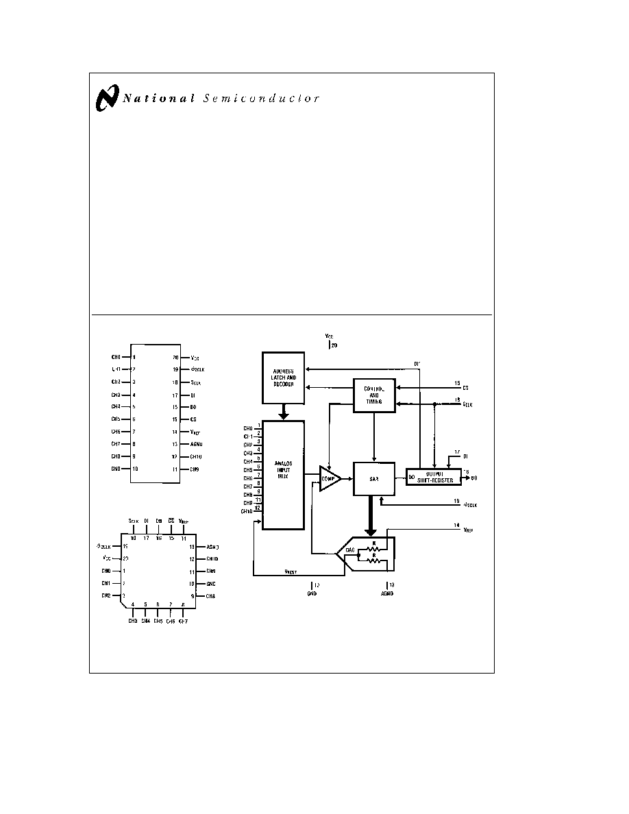
ADC0811 8-Bit Serial I O A D Converter
With 11-Channel Multiplexer
General Description
The ADC0811 is an 8-Bit successive approximation A D
converter with simultaneous serial I O The serial input con-
trols an analog multiplexer which selects from 11 input
channels or an internal half scale test voltage
An input sample-and-hold is implemented by a capacitive
reference ladder and sampled data comparator This allows
the input signal to vary during the conversion cycle
Separate serial I O and conversion clock inputs are provid-
ed to facilitate the interface to various microprocessors
Features
Y
Separate asynchronous converter clock and serial data
I O clock
Y
11-Channel multiplexer with 4-Bit serial address logic
Y
Built-in sample and hold function
Y
Ratiometric or absolute voltage referencing
Y
No zero or full-scale adjust required
Y
Internally addressable test voltage
Y
0V to 5V input range with single 5V power supply
Y
TTL MOS input output compatible
Y
0 3
standard width 20-pin dip or 20-pin molded chip
carrier
Key Specifications
Y
Resolution
8-Bits
Y
Total unadjusted error
g
LSB and
g
1LSB
Y
Single supply
5V
DC
Y
Low Power
15 mW
Y
Conversion Time
32 mS
Connection Diagrams
Dual-In-Line Package
TL H 5587 1
Top View
Molded Chip Carrier (PCC) Package
TL H 5587 2
Top View
Order Number ADC0811J N V
See NS Packages J20A N20A V20A
Use Ordering Information
Functional Diagram
TL H 5587 3
C1995 National Semiconductor Corporation
RRD-B30M115 Printed in U S A
Absolute Maximum Ratings
(Notes 1
2)
If Military Aerospace specified devices are required
please contact the National Semiconductor Sales
Office Distributors for availability and specifications
Supply Voltage (V
CC
)
6 5V
Voltage
Inputs and Outputs
b
0 3V to V
CC
a
0 3V
Input Current Per Pin (Note 3)
g
5mA
Total Package Input Current (Note 3)
g
20mA
Storage Temperature
b
65 C to
a
150 C
Package Dissipation at T
A
e
25 C
875 mW
Lead Temp (Soldering 10 seconds)
Dual-In-Line Package (plastic)
260 C
Dual-In-Line Package (ceramic)
300 C
Molded Chip Carrier Package
Vapor Phase (60 seconds)
215 C
Infrared (15 seconds)
220 C
ESD Susceptibility (Note 11)
2000V
Operating Ratings
(Notes 1
2)
Supply Voltage (V
CC
)
4 5 V
DC
to 6 0 V
DC
Temperature Range
T
MIN
s
T
A
s
T
MAX
ADC0811BCN ADC0811CCN
0 C
s
T
A
s
70 C
ADC0811BCV
b
40 C
s
T
A
s
85 C
ADC0811CCJ ADC0811CCV
b
40 C
s
T
A
s
85 C
Electrical Characteristics
The following specifications apply for V
CC
e
4 75V to 5 25V V
REF
e a
4 6V to (V
CC
a
0 1V) w
2 CLK
e
2 097 MHz unless
otherwise specified Boldface limits apply from T
MIN
to T
MAX
all other limits T
A
e
T
J
e
25 C
Parameter
Conditions
ADC0811CCJ
ADC0811BCN ADC0811BCV
Units
ADC0811CCN ADC0811CCV
Typical
Tested
Design
Typical
Tested
Design
(Note 6)
Limit
Limit
(Note 6)
Limit
Limit
(Note 7)
(Note 8)
(Note 7)
(Note 8)
CONVERTER AND MULTIPLEXER CHARACTERISTICS
Maximum Total
V
REF
e
5 00 V
DC
Unadjusted Error
(Note 4)
ADC0811BCN ADC0811BCV
g
g
LSB
ADC0811CCN ADC0811CCV
g
1
g
1
LSB
ADC0811CCJ
g
1
LSB
Minimum Reference
8
5
8
5
kX
Input Resistance
Maximum Reference
8
11
8
11
11
kX
Input Resistance
Maximum Analog Input Range
(Note 5)
V
CC
a
0 05
V
CC
a
0 05 V
CC
a
0 05
V
Minimum Analog Input Range
GND
b
0 05
GND
b
0 05 GND
b
0 05
V
On Channel Leakage Current
ADC0811BCJ CCJ BCN CCN
On Channel
e
5V
1000
400
1000
nA
BCV CCV
Off Channel
e
0V
ADC0811CJ BJ
1000
nA
ADC0811BCJ CCJ BCN CCN
On Channel
e
0V
b
1000
b
400
b
1000
nA
BCV CCV
Off Channel
e
5V
ADC0811BJ CJ
(Note 9)
b
1000
nA
Off Channel Leakage Current
ADC0811BCJ CCJ BCN CCN
On Channel
e
5V
b
1000
b
400
1000
nA
BCV CCV
Off Channel
e
0V
ADC0811CJ BJ
b
1000
nA
ADC0811BCJ CCJ BCN CCN
On Channel
e
0V
1000
400
1000
nA
BCV CCV
Off Channel
e
5V
ADC0811BJ CJ
(Note 9)
1000
nA
Minimum V
TEST
V
REF
e
V
CC
(Note 10)
Internal Test Voltage
CH 11 Selected
125
125
125
Counts
Maximum V
TEST
V
REF
e
V
CC
(Note 10)
Internal Test Voltage
CH 11 Selected
130
130
130
Counts
2
Electrical Characteristics
The following specifications apply for V
CC
e
4 75V to 5 25V V
REF
e a
4 6V to (V
CC
a
0 1V) w
2 CLK
e
2 097 MHz unless
otherwise specified Boldface limits apply from T
MIN
to T
MAX
all other limits T
A
e
T
J
e
25 C (Continued)
Parameter
Conditions
ADC0811CCJ
ADC0811BCN ADC0811BCV
Units
ADC0811CCN ADC0811CCV
Typical
Tested
Design
Typical
Tested
Design
(Note 6)
Limit
Limit
(Note 6)
Limit
Limit
(Note 7)
(Note 8)
(Note 7)
(Note 8)
DIGITAL AND DC CHARACTERISTICS
V
IN(1)
Logical ``1'' Input
V
CC
e
5 25V
2 0
2 0
2 0
V
Voltage (Min)
V
IN(0)
Logical ``0'' Input
V
CC
e
4 75V
0 8
0 8
0 8
V
Voltage (Max)
I
IN(1)
Logical ``1'' Input
V
IN
e
5 0V
0 005
2 5
0 005
2 5
2 5
m
A
Current (Max)
I
IN(0)
Logical ``0'' Input
V
IN
e
0V
b
0 005
b
2 5
b
0 005
2 5
b
2 5
m
A
Current (Max)
V
OUT(1)
Logical ``1''
V
CC
e
4 75V
Output Voltage (Min)
I
OUT
e b
360 mA
2 4
2 4
2 4
V
I
OUT
e b
10 mA
4 5
4 5
4 5
V
V
OUT(0)
Logical ``0''
V
CC
e
5 25V
0 4
0 4
0 4
V
Output Voltage (Max)
I
OUT
e
1 6 mA
I
OUT
TRI-STATE Output
V
OUT
e
0V
b
0 01
b
3
b
0 01
b
3
b
3
m
A
Current (Max)
V
OUT
e
5V
0 01
3
0 01
3
3
m
A
I
SOURCE
Output Source
V
OUT
e
0V
b
12
b
6 5
b
14
b
6 5
b
6 5
mA
Current (Min)
I
SINK
Output Sink Current (Min)
V
OUT
e
V
CC
18
8 0
16
8 0
8 0
mA
I
CC
Supply Current (Max)
CS
e
1 V
REF
Open
1
2 5
1
2 5
2 5
mA
I
REF
(Max)
V
REF
e
5V
0 7
1
0 7
1
1
mA
AC CHARACTERISTICS
Tested
Design
Parameter
Conditions
Typical
Limit
Limit
Units
(Note 6)
(Note 7)
(Note 8)
w
CLK
w
Clock Frequency
MIN
1 0
MHz
MAX
2 1
S
CLK
Serial Data Clock
MIN
5 0
KHz
Frequency
MAX
525
T
C
Conversion Process Time
MIN
Not Including MUX
48
w
cycles
Addressing and
MAX
Analog Input
64
Sampling Times
t
ACC
Access Time Delay From CS
MIN
1
w
cycles
Falling Edge to DO Data Valid
MAX
3
t
SET UP
Minimum Set up Time of CS Falling
4 w
2CLK
a
1
2 S
CLK
sec
Edge to S
CLK
Rising Edge
t
HCS
CS Hold Time After the Falling
0
ns
Edge of S
CLK
t
CS
Total CS Low Time
MIN
t
set-up
a
8 S
CLK
sec
MAX
t
CS
(min)
a
48 w
2CLK
sec
t
HDI
Minimum DI Hold Time from
0
ns
S
CLK
Rising Edge
t
HDO
Minimum DO Hold Time from S
CLK
R
L
e
k
10
ns
Falling Edge
C
L
e
pF
3
Electrical Characteristics
The following specifications apply for V
CC
e
4 75V to 5 25V V
REF
e a
4 6V to (V
CC
a
0 1V) w
2 CLK
e
2 097 MHz unless
otherwise specified Boldface limits apply from T
MIN
to T
MAX
all other limits T
A
e
T
J
e
25 C (Continued)
Typical
Tested
Design
Parameter
Conditions
(Note 6)
Limit
Limit
Units
(Note 7)
(Note 8)
AC CHARACTERISTICS
(Continued)
t
SDI
Minimum DI Set-up Time to S
CLK
200
400
ns
Rising Edge
t
DDO
Maximum Delay From S
CLK
R
L
e
30k
180
400
400
ns
Falling Edge to DO Data Valid
C
L
e
100 pF
t
TRI
Maximum DO Hold Time
R
L
e
3k
(CS Rising edge to DO
C
L
e
100 pF
90
150
150
ns
TRI-STATE)
t
CA
Analog
After Address Is Latched
4 S
CLK
a
1 ms
sec
Sampling Time
CS
e
Low
t
RDO
Maximum DO
R
L
e
30 kX
``TRI-STATE'' to ``HIGH'' State
75
150
150
ns
Rise Time
C
L
e
100 pf
``LOW'' to ``HIGH'' State
150
300
300
t
FDO
Maximum DO
R
L
e
30 kX
``TRI-STATE'' to ``LOW'' State
75
150
150
ns
Fall Time
C
L
e
100 pf
``HIGH'' to ``LOW'' State
150
300
300
C
IN
Maximum Input
Analog Inputs ANO AN10 and V
REF
11
55
pF
Capacitance
All Others
5
15
Note 1
Absolute Maximum Ratings indicate limits beyond which damage to the device may occur DC and AC electrical specifications do not apply when operating
the device beyond its specified operating conditions
Note 2
All voltages are measured with respect to ground
Note 3
Under over voltage conditions (V
IN
k
0V and V
IN
l
V
CC
) the maximum input current at any one pin is
g
5 mA If the voltage at more than one pin exceeds
V
CC
a
3V the total package current must be limited to 20 mA For example the maximum number of pins that can be over driven at the maximum current level of
g
5 mA is four
Note 4
Total unadjusted error includes offset full-scale linearity multiplexer and hold step errors
Note 5
Two on-chip diodes are tied to each analog input which will forward-conduct for analog input voltages one diode drop below ground or one diode drop
greater than V
CC
supply Be careful during testing at low V
CC
levels (4 5V) as high level analog inputs (5V) can cause this input diode to conduct especially at
elevated temperatures and cause errors for analog inputs near full-scale The spec allows 50 mV forward bias of either diode This means that as long as the
analog V
IN
does not exceed the supply voltage by more than 50 mV the output code will be correct To achieve an absolute 0 V
DC
to 5 V
DC
input voltage range will
therefore require a minimum supply voltage of 4 950 V
DC
over temperature variations initial tolerance and loading
Note 6
Typicals are at 25 C and represent most likely parametric norm
Note 7
Guaranteed and 100% production tested under worst case condition
Note 8
Guaranteed but not 100% production tested These limits are not used to calculate outgoing quality levels
Note 9
Channel leakage current is measured after the channel selection
Note 10
1 count
e
V
REF
256
Note 11
Human body model 100 pF discharged through a 1 5 kX resistor
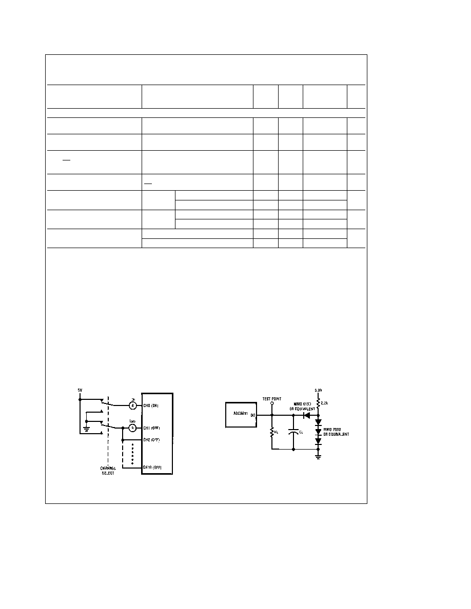
Test Circuits
Leakage Current
TL H 5587 17
D0 Except ``TRI-STATE''
TL H 5587 6
4
Test Circuits
(Continued)
t
TRI
``TRI-STATE''
TL H 5587 22
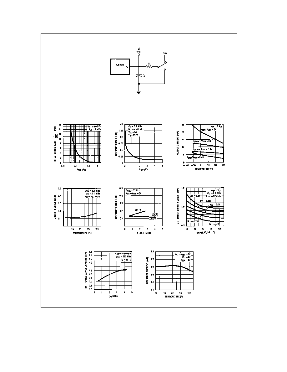
Typical Performance Characteristics
Unadjusted Offset Error vs
V
REF
Voltage
Linearity Error vs V
REF
Voltage
Output Current vs
Temperature
Linearity vs Temperature
Linearity vs w
2
Clock
Frequency
Power Supply Current
vs Temperature
Power Supply Current vs
w
2
Clock Frequency
Resistive Ladder Reference
Current vs Temperature
TL H 5587 16
5