 | –≠–ª–µ–∫—Ç—Ä–æ–Ω–Ω—ã–π –∫–æ–º–ø–æ–Ω–µ–Ω—Ç: ADC0817C | –°–∫–∞—á–∞—Ç—å:  PDF PDF  ZIP ZIP |
ADC0816/ADC0817
8-Bit µP Compatible A/D Converters
with 16-Channel Multiplexer
General Description
The ADC0816, ADC0817 data acquisition component is a
monolithic CMOS device with an 8-bit analog-to-digital con-
verter, 16-channel multiplexer and microprocessor compat-
ible control logic. The 8-bit A/D converter uses successive
approximation as the conversion technique. The converter
features a high impedance chopper stabilized comparator, a
256R voltage divider with analog switch tree and a succes-
sive approximation register. The 16-channel multiplexer can
directly access any one of 16-single-ended analog signals,
and provides the logic for additional channel expansion.
Signal conditioning of any analog input signal is eased by
direct access to the multiplexer output, and to the input of the
8-bit A/D converter.
The device eliminates the need for external zero and
full-scale adjustments. Easy interfacing to microprocessors
is provided by the latched and decoded multiplexer address
inputs and latched TTL TRI-STATE
Æ
outputs.
The design of the ADC0816, ADC0817 has been optimized
by incorporating the most desirable aspects of several A/D
conversion techniques. The ADC0816, ADC0817 offers high
speed, high accuracy, minimal temperature dependence,
excellent long-term accuracy and repeatability, and con-
sumes minimal power. These features make this device
ideally suited to applications from process and machine
control to consumer and automotive applications. For similar
performance in an 8-channel, 28-pin, 8-bit A/D converter,
see the ADC0808, ADC0809 data sheet. (See AN-258 for
more information.)
Features
n
Easy interface to all microprocessors
n
Operates ratiometrically or with 5 V
DC
or analog span
adjusted voltage reference
n
16-channel multiplexer with latched control logic
n
Outputs meet TTL voltage level specifications
n
0V to 5V analog input voltage range with single 5V
supply
n
No zero or full-scale adjust required
n
Standard hermetic or molded 40-pin DIP package
n
Temperature range -40∞C to +85∞C or -55∞C to +125∞C
n
Latched TRI-STATE output
n
Direct access to "comparator in" and "multiplexer out" for
signal conditioning
n
ADC0816 equivalent to MM74C948
n
ADC0817 equivalent to MM74C948-1
Key Specifications
n
Resolution
8 Bits
n
Total Unadjusted Error
±
1
/
2
LSB and
±
1 LSB
n
Single Supply
5 V
DC
n
Low Power
15 mW
n
Conversion Time
100 µs
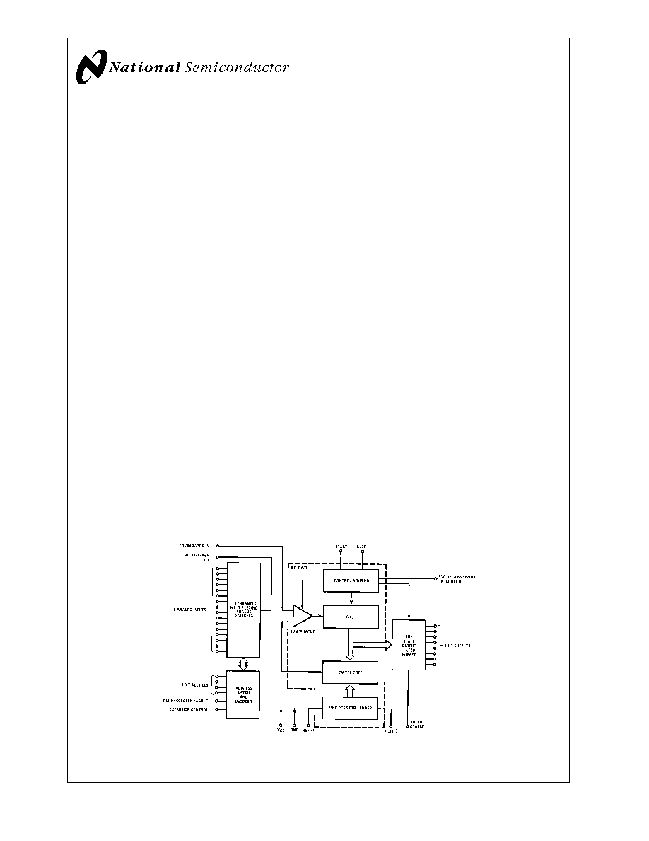
Block Diagram
DS005277-1
July 1999
ADC0816/ADC0817
8-Bit
µP
Compatible
A/D
Converters
with
16-Channel
Multiplexer
© 2001 National Semiconductor Corporation
DS005277
www.national.com
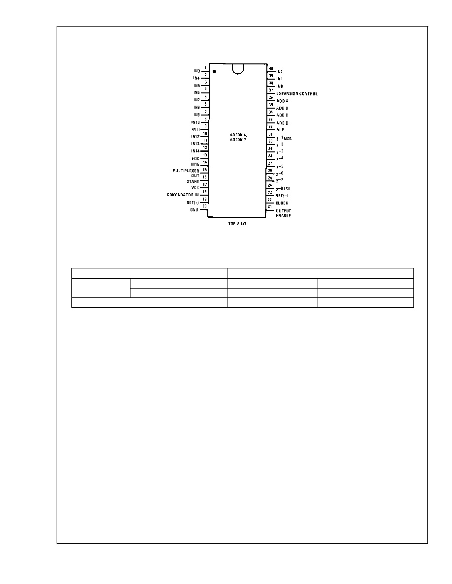
Connection Diagram
Ordering Information
TEMPERATURE RANGE
-40∞C to +85∞C
Error
±
1
/
2
Bit Unadjusted
ADC0816CCN
ADC0816CCJ
±
1 Bit Unadjusted
ADC0817CCN
Package Outline
N40A Molded DIP
J40A Hermetic DIP
Dual-In-Line Package
DS005277-6
Order Number ADC0816CCN or ADC0817CCN
See NS Package Number N40A
ADC0816/ADC0817
www.national.com
2
Absolute Maximum Ratings
(Notes 1, 2)
If Military/Aerospace specified devices are required,
please contact the National Semiconductor Sales Office/
Distributors for availability and specifications.
Supply Voltage (V
CC
) (Note 3)
6.5V
Voltage at Any Pin
-0.3V to (V
CC
+0.3V)
Except Control Inputs
Voltage at Control Inputs
-0.3V to 15V
(START, OE, CLOCK, ALE, EXPANSION CONTROL,
ADD A, ADD B, ADD C, ADD D)
Storage Temperature Range
-65∞C to + 150∞C
Package Dissipation at T
A
= 25∞C
875 mW
Lead Temp. (Soldering, 10 seconds)
Dual-In-Line Package (Plastic)
260∞C
Molded Chip Carrier Package
Vapor Phase (60 seconds)
215∞C
Infrared (15 seconds)
220∞C
ESD Susceptibility (Note 9)
400V
Operating Conditions
(Notes 1, 2)
Temperature Range (Note 1)
T
MIN
T
A
T
MAX
ADC0816CCN, ADC0817CCN
-40∞C
T
A
+85∞C
Range of V
CC
(Note 1)
4.5 V
DC
to 6.0 V
DC
Voltage at Any Pin
0V to V
CC
Except Control Inputs
Voltage at Control Inputs
0V to 15V
(START, OE, CLOCK, ALE, EXPANSION CONTROL,
ADD A, ADD B, ADD C, ADD D)
Electrical Characteristics
Converter Specifications: V
CC
=5 V
DC
= V
REF(+)
, V
REF(-)
=GND, V
IN
=V
COMPARATOR IN,
T
MIN
T
MAX
and f
CLK
= 640 kHz unless
otherwise stated.
Symbol
Parameter
Conditions
Min
Typ
Max
Units
ADC0816
Total Unadjusted Error
25∞C
±
1
/
2
LSB
(Note 5)
T
MIN
to T
MAX
±
3
/
4
LSB
ADC0817
Total Unadjusted Error
0∞C to 70∞C
±
1
LSB
(Note 5)
T
MIN
to T
MAX
±
1
1
/
4
LSB
Input Resistance
From Ref(+) to Ref(-)
1.0
4.5
k
Analog Input Voltage Range
(Note 4) V(+) or V(-)
GND-0.10
V
CC
+0.10
V
DC
V
REF(+)
Voltage, Top of Ladder
Measured at Ref(+)
V
CC
V
CC
+0.1
V
Voltage, Center of Ladder
V
CC
/2-0.1
V
CC
/2
V
CC
/2+0.1
V
V
REF(-)
Voltage, Bottom of Ladder
Measured at Ref(-)
-0.1
0
V
Comparator Input Current
f
c
=640 kHz, (Note 6)
-2
±
0.5
2
µA
Electrical Characteristics
Digital Levels and DC Specifications: ADC0816CCN, ADC0817CCN -- 4.75V
V
CC
5.25V, -40∞C
T
A
+85∞C unless other-
wise noted.
Symbol
Parameter
Conditions
Min
Typ
Max
Units
ANALOG MULTIPLEXER
R
ON
Analog Multiplexer ON
(Any Selected Channel)
Resistance
T
A
=25∞C, R
L
=10k
1.5
3
k
T
A
=85∞C
6
k
T
A
=125∞C
9
k
R
ON
ON Resistance Between Any
(Any Selected Channel)
75
2 Channels
R
L
=10k
I
OFF+
OFF Channel Leakage Current
V
CC
=5V, V
IN
=5V,
T
A
=25∞C
10
200
nA
T
MIN
to T
MAX
1.0
µA
I
OFF(-)
OFF Channel Leakage Current
V
CC
=5V, V
IN
=0,
T
A
=25∞C
-200
nA
T
MIN
to T
Max
-1.0
µA
ADC0816/ADC0817
www.national.com
3

Electrical Characteristics
(Continued)
Digital Levels and DC Specifications: ADC0816CCN, ADC0817CCN -- 4.75V
V
CC
5.25V, -40∞C
T
A
+85∞C unless other-
wise noted.
Symbol
Parameter
Conditions
Min
Typ
Max
Units
CONTROL INPUTS
V
IN(1)
Logical "1" Input Voltage
V
CC
-1.5
V
V
IN(0)
Logical "0" Input Voltage
1.5
V
I
IN(1)
Logical "1" Input Current
V
IN
=15V
1.0
µA
(The Control Inputs)
I
IN(0)
Logical "0" Input Current
V
IN
=0
-1.0
µA
(The Control Inputs)
I
CC
Supply Current
f
CLK
=640 kHz
0.3
3.0
mA
DATA OUTPUTS AND EOC (INTERRUPT)
V
OUT(1)
Logical "1" Output Voltage
I
O
=-360 µA, T
A
=85∞C
V
CC
-0.4
V
I
O
=-300 µA, T
A
=125∞C
V
OUT(0)
Logical "0" Output Voltage
I
O
=1.6 mA
0.45
V
V
OUT(0)
Logical "0" Output Voltage EOC
I
O
=1.2 mA
0.45
V
I
OUT
TRI-STATE Output Current
V
O
=V
CC
3.0
µA
V
O
=0
-3.0
µA
Electrical Characteristics
Timing Specifications: V
CC
=V
REF(+)
=5V, V
REF(-)
=GND, t
r
=t
f
=20 ns and T
A
=25∞C unless otherwise noted.
Symbol
Parameter
Conditions
Min
Typ
Max
Units
t
WS
Minimum Start Pulse Width
(
Figure 5) (Note 7)
100
200
ns
t
WALE
Minimum ALE Pulse Width
(
Figure 5)
100
200
ns
t
s
Minimum Address Set-Up Time
(
Figure 5)
25
50
ns
T
H
Minimum Address Hold Time
(
Figure 5)
25
50
ns
t
D
Analog MUX Delay Time
R
S
=O
(
Figure 5)
1
2.5
µs
from ALE
t
H1
, t
H0
OE Control to Q Logic State
C
L
=50 pF, R
L
=10k (
Figure 8)
125
250
ns
t
1H,
t
0H
OE Control to Hi-Z
C
L
=10 pF, R
L
=10k (
Figure 8)
125
250
ns
t
C
Conversion Time
f
c
=640 kHz, (
Figure 5) (Note 8)
90
100
116
µs
f
c
Clock Frequency
10
640
1280
kHz
t
EOC
EOC Delay Time
(
Figure 5)
0
8+2µs
Clock
Periods
C
IN
Input Capacitance
At Control Inputs
10
15
pF
C
OUT
TRI-STATE Output
At TRI-STATE Outputs (Note 8)
10
15
pF
Capacitance
Note 1: Absolute Maximum Ratings indicate limits beyond which damage to the device may occur. DC and AC electrical specifications do not apply when operating
the device beyond its specified operating conditions.
Note 2: All voltages are measured with respect to GND, unless otherwise specified.
Note 3: A zener diode exists, internally, from V
CC
to GND and has a typical breakdown voltage of 7 V
DC
.
Note 4: Two on-chip diodes are tied to each analog input which will forward conduct for analog input voltages one diode drop below ground or one diode drop
greater than the V
CC
supply. The spec allows 100 mV forward bias of either diode. This means that as long as the analog V
IN
does not exceed the supply voltage
by more than 100 mV, the output code will be correct. To achieve an absolute 0 V
DC
to 5 V
DC
input voltage range will therefore require a minimum supply voltage
of 4.900 V
DC
over temperature variations, initial tolerance and loading.
Note 5: Total unadjusted error includes offset, full-scale, and linearity errors. See
Figure 3
. None of these A/Ds requires a zero or full-scale adjust. However, if an
all zero code is desired for an analog input other than 0.0V, or if a narrow full-scale span exists (for example: 0.5V to 4.5V full-scale) the reference voltages can be
adjusted to achieve this. See
Figure 13
.
Note 6: Comparator input current is a bias current into or out of the chopper stabilized comparator. The bias current varies directly with clock frequency and has
little temperature dependence (
Figure 6
). See paragraph 4.0.
Note 7: If start pulse is asynchronous with converter clock or if f
c
>
640 kHz, the minimum start pulse width is 8 clock periods plus 2 µs. For synchronous operation
at f
c
640 kHz take start high within 100 ns of clock going low.
Note 8: The outputs of the data register are updated one clock cycle before the rising edge of EOC.
Note 9: Human body model, 100 pF discharged through a 1.5 k
resistor.
ADC0816/ADC0817
www.national.com
4
Functional Description
Multiplexer: The device contains a 16-channel single-ended
analog signal multiplexer. A particular input channel is se-
lected by using the address decoder.
Table 1 shows the input
states for the address line and the expansion control line to
select any channel. The address is latched into the decoder
on the low-to-high transition of the address latch enable
signal.
TABLE 1.
Selected
Address Line
Expansion
Analog Channel
D
C
B
A
Control
IN0
L
L
L
L
H
IN1
L
L
L
H
H
IN2
L
L
H
L
H
IN3
L
L
H
H
H
IN4
L
H
L
L
H
IN5
L
H
L
H
H
IN6
L
H
H
L
H
IN7
L
H
H
H
H
IN8
H
L
L
L
H
IN9
H
L
L
H
H
IN10
H
L
H
L
H
IN11
H
L
H
H
H
IN12
H
H
L
L
H
IN13
H
H
L
H
H
IN14
H
H
H
L
H
IN15
H
H
H
H
H
All Channels OFF
X
X
X
X
L
X=don't care
Additional single-ended analog signals can be multiplexed to
the A/D converter by disabling all the multiplexer inputs using
the expansion control. The additional external signals are
connected to the comparator input and the device ground.
Additional signal conditioning (i.e., prescaling, sample and
hold, instrumentation amplification, etc.) may also be added
between the analog input signal and the comparator input.
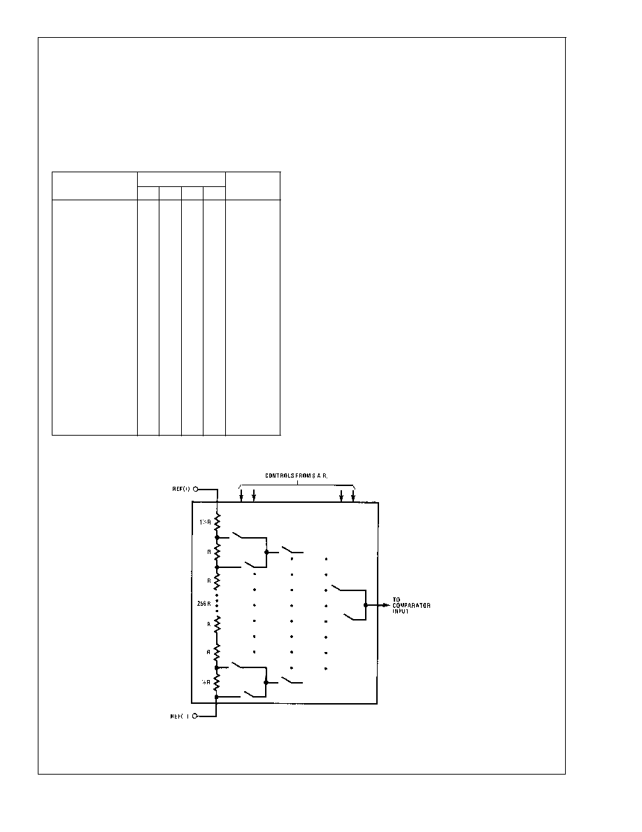
CONVERTER CHARACTERISTICS
The Converter
The heart of this single chip data acquisition system is its
8-bit analog-to-digital converter. The converter is designed to
give fast, accurate, and repeatable conversions over a wide
range of temperatures. The converter is partitioned into 3
major sections: the 256R ladder network, the successive
approximation register, and the comparator. The converter's
digital outputs are positive true.
The 256R ladder network approach
Figure 1 was chosen
over the conventional R/2R ladder because of its inherent
monotonicity, which guarantees no missing digital codes.
Monotonicity is particularly important in closed loop feedback
control systems. A non-monotonic relationship can cause
oscillations that will be catastrophic for the system. Addition-
ally, the 256R network does not cause load variations on the
reference voltage.
The bottom resistor and the top resistor of the ladder net-
work in
Figure 1 are not the same value as the remainder of
the network. The difference in these resistors causes the
output characteristic to be symmetrical with the zero and
full-scale points of the transfer curve. The first output transi-
tion occurs when the analog signal has reached +
1
/
2
LSB
and succeeding output transitions occur every 1 LSB later up
to full-scale.
DS005277-2
FIGURE 1. Resistor Ladder and Switch Tree
ADC0816/ADC0817
www.national.com
5