TL H 5607
ADC0833
8-Bit
Serial
IO
AD
Converter
with
4-Channel
Multiplexer
December 1994
ADC0833 8-Bit Serial I O A D Converter
with 4-Channel Multiplexer
General Description
The ADC0833 series is an 8-bit successive approximation
A D converter with a serial I O and configurable input multi-
plexer with 4 channels The serial I O is configured to com-
ply with the NSC MICROWIRE
TM
serial data exchange stan-
dard for easy interface to the COPS
TM
family of processors
as well as with standard shift registers or mPs
The 4-channel multiplexer is software configured for single-
ended or differential inputs when channel assigned by a 4-
bit serial word
The differential analog voltage input allows increasing the
common-mode rejection and offsetting the analog zero in-
put voltage value In addition the voltage reference input
can be adjusted to allow encoding any smaller analog volt-
age span to the full 8 bits of resolution
Key Specifications
Y
Resolution
8 Bits
Y
Total Unadjusted Error
g
LSB and
g
1 LSB
Y
Single Supply
5 V
DC
Y
Low Power
23 mW
Y
Conversion Time
32 ms
Features
Y
NSC MICROWIRE compatible � direct interface to COPS
family processors
Y
Easy interface to all microprocessors
or operates
``stand alone''
Y
Works with 2 5V (LM336) voltage reference
Y
No full-scale or zero adjust required
Y
Differential analog voltage inputs
Y
4-channel analog multiplexer
Y
Shunt regulator allows operation with high voltage
supplies
Y
0V to 5V input range with single 5V power supply
Y
Remote operation with serial digital data link
Y
TTL MOS input output compatible
Y
0 3
standard width 14-pin DIP package
Connection and Functional Diagrams
Dual-In-Line Package (J and N)
TL H 5607 � 14
Top View
Order Number ADC0833CCJ
ADC0833BCN or ADC0833CCN
See NS Package Number
J14A or N14A
TL H 5607 � 1
COPS
TM
and MICROWIRE
TM
are trademarks of National Semiconductor Corporation
TRI-STATE
is a registered trademark of National Semiconductor Corporation
C1995 National Semiconductor Corporation
RRD-B30M115 Printed in U S A
Absolute Maximum Ratings
(Notes 1
2)
If Military Aerospace specified devices are required
please contact the National Semiconductor Sales
Office Distributors for availability and specifications
Current into V
a
(Note 3)
15 mA
Supply Voltage V
CC
(Note 3)
6 5V
Voltage
Logic Inputs
b
0 3V to V
CC
a
0 3V
Analog Inputs
b
0 3V to V
CC
a
0 3V
Input Current per Pin (Note 4)
g
5 mA
Package Input Current (Note 4)
g
20 mA
Storage Temperature
b
65 C to
a
150 C
Package Dissipation at
T
A
e
25 C (Board Mount)
0 8W
Lead Temperature (Soldering 10 sec )
Dual-In-Line Package (Plastic)
260 C
Dual-In-Line Package (Ceramic)
300 C
ESD Susceptibility (Note 5)
2000V
Operating Conditions
(Notes 1
2)
Supply Voltage V
CC
4 5 V
DC
to 6 3 V
DC
Temperature Range
T
MIN
s
T
A
s
T
MAX
ADC0833CCJ
b
40 C
s
T
A
s
85 C
ADC0833BCN ADC0833CCN
0 C
s
T
A
s
70 C
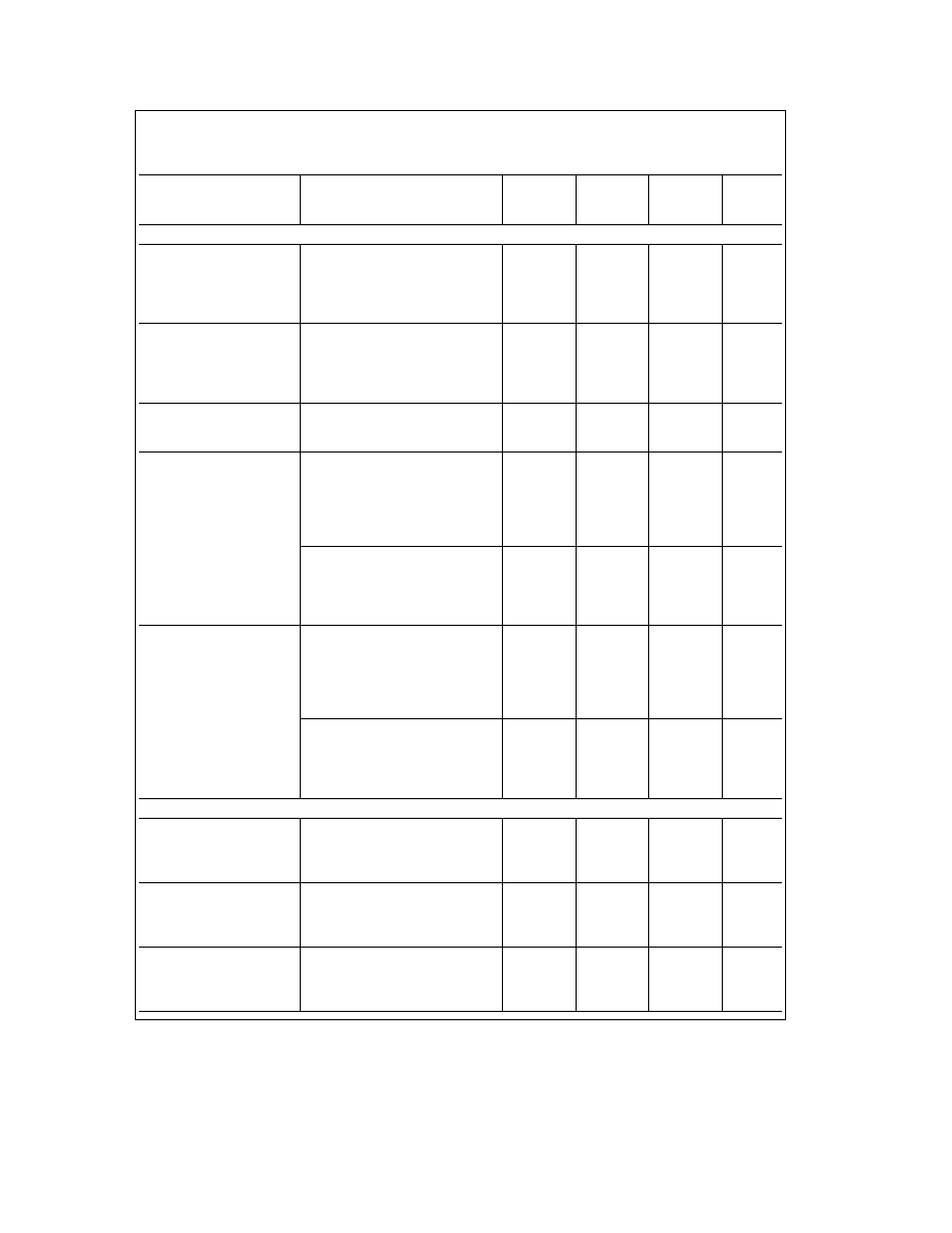
Electrical Characteristics
The following specifications apply for V
CC
e
V
a
e
5V f
CLK
e
250 kHz and
V
REF
2
s
(V
CC
a
0 1V) unless otherwise specified Boldface limits apply from T
MIN
to T
MAX
all other limits
T
A
e
T
j
e
25 C
Typ
Tested
Design
Parameter
Conditions
(Note 6)
Limit
Limit
Units
(Note 7)
(Note 8)
CONVERTER AND MULTIPLEXER CHARACTERISTICS
Total Unadjusted Error
V
REF
2 Forced to 2 500 V
DC
ADC0833BCN
g
g
LSB
ADC0833CCN
g
1
g
1
LSB
ADC0833CCJ
g
1
LSB
Minimum Total Ladder
Resistance (Note 9)
ADC0833CCJ
7 0
2 6
kX
ADC0833BCN CCN
7 0
2 6
2 6
kX
Maximum Total Ladder
Resistance (Note 9)
ADC0833CCJ
7 0
11 8
kX
ADC0833BCN CCN
7 0
10 8
11 8
kX
Minimum Common-Mode
All MUX Inputs and COM Input
Input Range (Note 10)
ADC0833CCJ
GND
b
0 05
V
ADC0833BCN CCN
GND
b
0 05
GND
b
0 05
V
Maximum Common-Mode
All MUX Inputs and COM Input
Input Range (Note 10)
ADC0833CCJ
V
CC
a
0 05
V
ADC0833BCN CCN
V
CC
a
0 05
V
CC
a
0 05
V
DC Common-Mode Error
ADC0833CCJ
g
g
LSB
ADC0833BCN CCN
g
g
g
LSB
Change In Zero
15mA Into V
a
Error From V
CC
e
5V
V
CC
e
N C
To Internal Zener
V
REF
2
e
2 500V
Operation (Note 3)
ADC0833CCJ
1
LSB
ADC0833BCN CCN
1
1
LSB
2

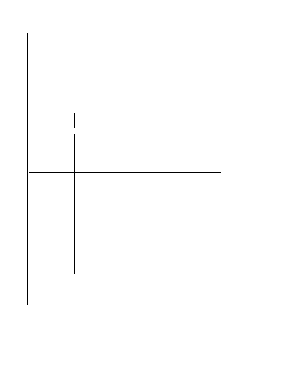
AC Electrical Characteristics
The following specifications apply for V
CC
e
V
a
e
5V and t
r
e
t
f
e
20 ns
unless otherwise specified These limits apply for T
A
e
T
j
e
25 C
Typ
Tested
Design
Parameter
Conditions
(Note 6)
Limit
Limit
Units
(Note 7)
(Note 8)
f
CLK
Clock Frequency
Min
10
kHz
Max
400
kHz
T
C
Conversion Time
Not including MUX Addressing Time
8
1 f
CLK
Clock Duty Cycle (Note 12)
Min
40
%
Max
60
%
t
SET-UP
CS Falling Edge or
250
ns
Data Input Valid to CLK
Rising Edge
t
HOLD
Data Input Valid
90
ns
after CLK Rising Edge
t
pd1
t
pd0
CLK Falling
C
L
e
100 pF
Edge to Output Data Valid
Data MSB First
650
1500
ns
(Note 13)
Data LSB First
250
600
ns
t
1H
t
OH
Rising Edge of CS
C
L
e
10 pF R
L
e
10k
125
250
ns
to Data Output and SARS
C
L
e
100 pF R
L
e
2k
500
ns
Hi-Z
(see TRI-STATE Test Circuits)
C
IN
Capacitance of Logic
5
pF
Input
C
OUT
Capacitance of Logic
5
pF
Outputs
Note 1
Absolute Maximum Ratings indicate limits beyond which damage to the device may occur DC and AC electrical specifications do not apply when operating
the device beyond its specified operating conditions
Note 2
All voltages are measured with respect to the ground pins
Note 3
Internal zener diodes (approx 7V) are connected from V
a
to GND and V
CC
to GND The zener at V
a
can operate as a shunt regulator and is connected to
V
CC
via a conventional diode Since the zener voltage equals the A D's breakdown voltage the diode insures that V
CC
will be below breakdown when the device is
powered from V
a
Functionality is therefore guaranteed for V
a
operation even though the resultant voltage at V
CC
may exceed the specified Absolute Max of
6 5V It is recommended that a resistor be used to limit the max current into V
a
Note 4
When the input voltage (V
IN
) at any pin exceeds the power supply rails (V
IN
k
V
b
or V
IN
l
V
a
) the absolute value of current at that pin should be limited
to 5 mA or less The 20 mA package input current limits the number of pins that can exceed the power supply boundaries with a 5 mA current limit to four
Note 5
Human body model 100 pF discharged through a 1 5 kX resistor
Note 6
Typicals are at 25 C and represent most likely parametric norm
Note 7
Tested limits are guaranteed to National's AOQL (Average Outgoing Quality Level)
Note 8
Design limits are guaranteed but not 100% tested These limits are not used to calculate outgoing quality levels
Note 9
See Applications section 3 0
Note 10
For V
IN
(
b
)
t
V
IN
(
a
) the digital output code will be 0000 0000 Two on-chip diodes are tied to each analog input (see Block Diagram) which will forward
conduct for analog input voltages one diode drop below ground or one diode drop greater than the V
CC
supply Be careful during testing at low V
CC
levels (4 5V)
as high level analog inputs (5V) can cause this input diode to conduct
especially at elevated temperatures and cause errors for analog inputs near full-scale The
spec allows 50 mV forward bias of either diode This means that as long as the analog V
IN
or V
REF
does not exceed the supply voltage by more than 50 mV the
output code will be correct To achieve an absolute 0 V
DC
to 5 V
DC
input voltage range will therefore require a minimum supply voltage of 4 950 V
DC
over
temperature variations initial tolerance and loading
Note 11
Leakage current is measured with the clock not switching
Note 12
A 40% to 60% clock duty cycle range insures proper operation at all clock frequencies In the case that an available clock has a duty cycle outside of
these limits the minimum time the clock is high or the minimum time the clock is low must be at least 1ms The maximum time the clock can be high is 60 ms The
clocked can be stopped when low so long as the analog input voltage remains stable
Note 13
Since data MSB first is the output of the comparator used in the successive approximation loop an additional delay is built in (see Block Diagram) to
allow for comparator response time
5