ADC0851 and ADC0858 8-Bit Analog Data Acquisition and Monitoring Systems
TL H 11021
ADC0851
and
ADC0858
8-Bit
Analog
Data
Acquisition
and
Monitoring
Systems
January 1995
ADC0851 and ADC0858 8-Bit Analog Data
Acquisition and Monitoring Systems
General Description
The ADC0851 and ADC0858 are 2 and 8 input analog data
acquisition systems They can function as conventional mul-
tiple input A D converters automatic scanning A D convert-
ers or programmable analog ``watchdog'' systems
In
``watchdog'' mode they monitor analog inputs and deter-
mine whether these inputs are inside or outside user pro-
grammed window limits This monitoring process takes
place independent of the host processor When any input
falls outside of its programmed window limits an interrupt is
automatically generated which flags the processor the chip
can then be interrogated as to exactly which channels
crossed which limits
The advantage of this approach is that its frees the proces-
sor from having to frequently monitor analog variables It
can consequently save having to insert many A D subrou-
tine calls throughout real time application code In control
systems where many variables are continually being moni-
tored this can significantly free up the processor especially
if the variables are DC or slow varying signals
The Auto A D conversion feature allows the device to scan
through selected input channels performing an A D conver-
sion on each channel without the need to select a new
channel after each conversion
Applications
Y
Instrumentation monitoring and process control
Y
Digitizing automotive sensor signals
Y
Embedded diagnostics
Key Specifications
Y
Resolution
8 Bits
Y
Total error
g
LSB or
g
1 LSB
Y
Low power
50 mW
Y
Conversion time
18 ms Channel
Y
Limit comparison time
2 ms Limit
Features
Y
Watchdog operation signals processor when any
channel is outside user programmed window limits
Y
Frees microprocessor from continually monitoring
analog signals and simplifies applications software
Y
2 (ADC0851) or 8 (ADC0858) analog input channels
Y
Single ended or differential input pairs
Y
COM input for DC offsetting of input voltage
Y
4 (ADC0851) and 16 (ADC0858) 8-bit programmable
limits
Y
NSC MICROWIRE
TM
interface
Y
Power fail detection
Y
Auto A D conversion feature
Y
Single 5V supply
Y
Window limits are user programmable via serial inter-
face
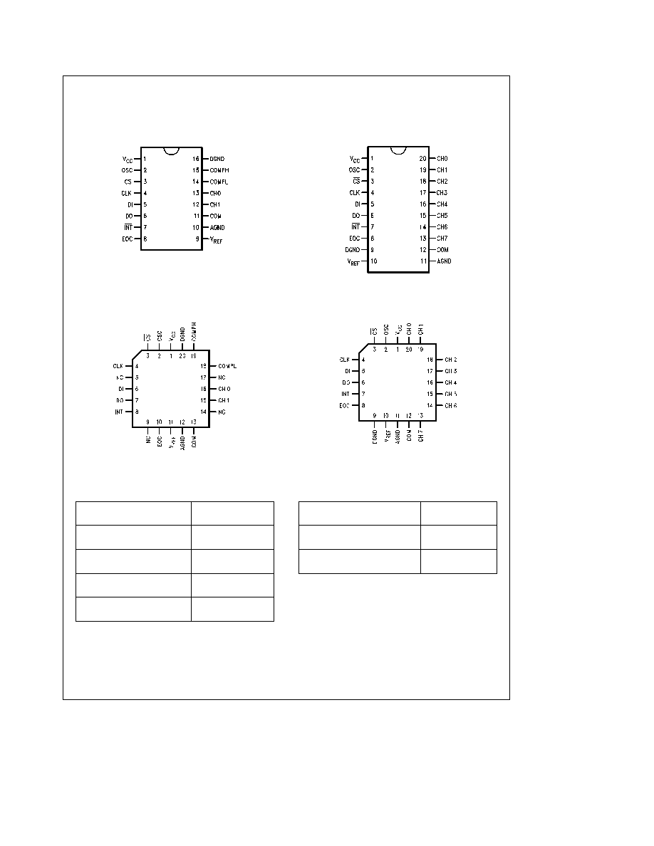
Simplified Block Diagram
TL H 11021 � 22
FIGURE 1
TRI-STATE
is a registered trademark of National Semiconductor Corporation
MICROWIRE
TM
is a trademark of National Semiconductor Corporation
C1995 National Semiconductor Corporation
RRD-B30M75 Printed in U S A
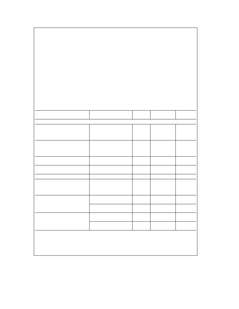
Connection Diagrams
ADC0851
2-Channel MUX
Dual-In-Line Package
TL H 11021 � 1
Top View
ADC0858
8-Channel MUX
Dual-In-Line Package
TL H 11021 � 2
Top View
ADC0851 PLCC Package
TL H 11021 � 3
Top View
ADC0858 PLCC Package
TL H 11021 � 4
Top View
Ordering Information
Industrial
Package
(
b
40 C
s
T
A
s
a
85 C)
ADC0851BIN
N16E 16-Pin
ADC0851CIN
Plastic DIP
ADC0858BIN
N20A 20-Pin
ADC0858CIN
Plastic DIP
ADC0851BIV
V20A 20-Lead
ADC0851CIV
PLCC
ADC0858BIV
V20A 20-Lead
ADC0858CIV
PLCC
Military
Package
(
b
55 C
s
T
A
s
a
125 C)
ADC0851CMJ 883
J16A 16-Pin
Ceramic DIP
ADC0858CMJ 883
J20A 20-Pin
Ceramic DIP
2
Absolute Maximum Ratings
(Notes 1
2)
If Military Aerospace specified devices are required
please contact the National Semiconductor Sales
Office Distributors for availability and specifications
Supply Voltage V
CC
6 5V
Voltage at Logic and Analog
Inputs (Note 3)
b
0 3V to V
CC
a
0 3V
Input Current per Pin
g
5 mA
Input Current per Package
g
20 mA
Storage Temperature
b
65 C to
a
150 C
Package Dissipation
500 mW
at T
A
e a
25 C (Board Mount)
800 mW
Lead Temperature (Soldering 10 Sec )
Dual-In-Line (Plastic)
a
260 C
Dual-In-Line (Ceramic)
a
300 C
ESD Susceptibility (Note 4)
2000V
Operating Ratings
(Notes 1
2)
Supply Voltage V
CC
4 5V to 5 5V
Temperature Range
T
MIN
s
T
A
s
T
MAX
ADC0858CMJ 883
b
55 C
s
T
A
s
a
125 C
ADC0851CMJ 883
b
55 C
s
T
A
s
a
125 C
ADC0858BIN ADC0858CIN
b
40 C
s
T
A
s
a
85 C
ADC0851BIN ADC0851CIN
b
40 C
s
T
A
s
a
85 C
ADC0858BIV ADC0858CIV
b
40 C
s
T
A
s
a
85 C
ADC0851BIV ADC0851CIV
b
40 C
s
T
A
s
a
85 C
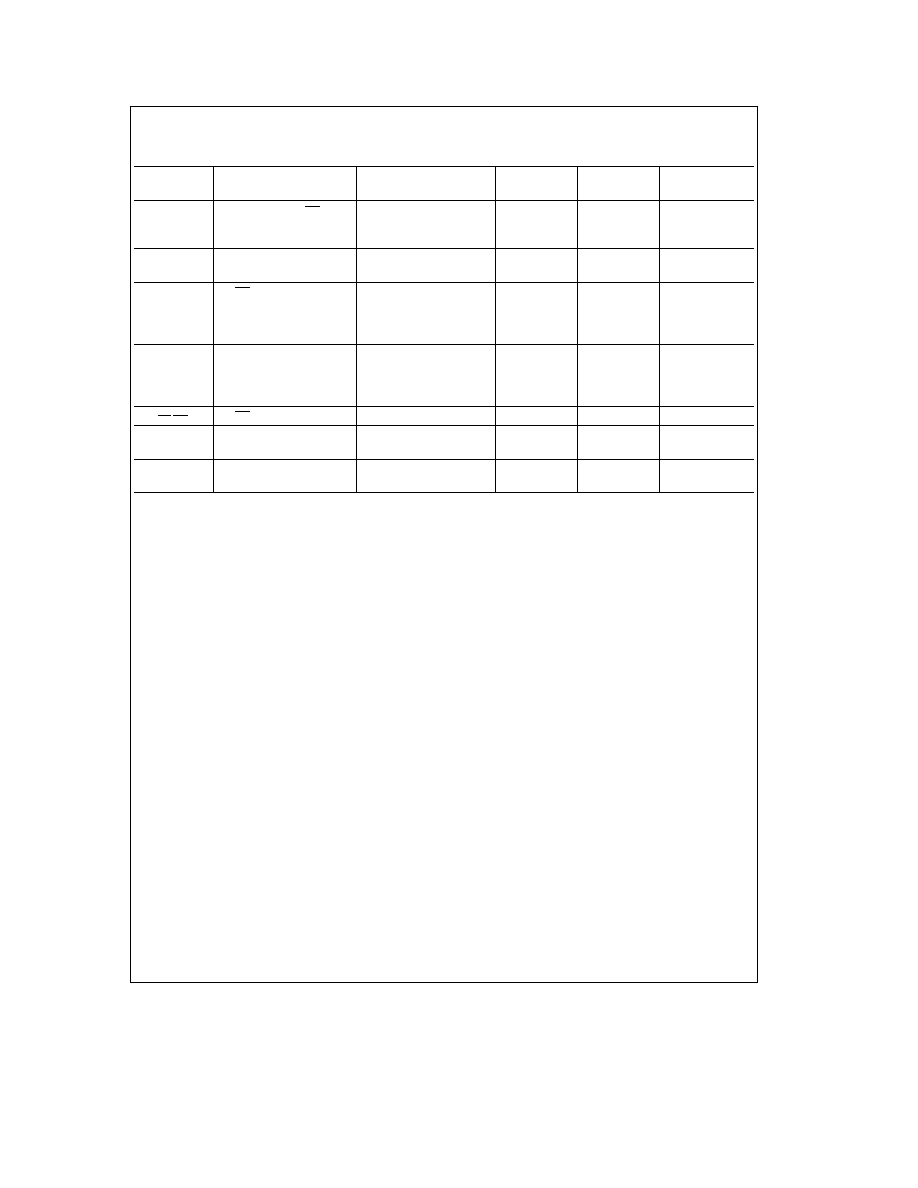
DC Electrical Characteristics
The following specifications apply for V
CC
e a
5 V
DC
V
REF
e a
4 5 V
DC
AGND
e
DGND
e
0V and f
OSC
e
1 MHz (R
ext
e
3 16 kX C
ext
e
170 pF) unless otherwise specified Boldface limits apply for T
A
e
T
J
e
T
MIN
to T
MAX
all other limits apply
at T
A
e
T
J
e a
25 C
Parameter
Conditions
Typical
Limit
Units
(Note 5)
(Note 6)
(Limits)
CONVERTER AND MULTIPLEXER CHARACTERISTICS
Total Unadjusted Error (Note 7)
ADC0851 8 BIN ADC0851 8 BIV
g
LSB (Max)
ADC0851 8 CIN ADC0851 8 CMJ
g
1
LSB (Max)
ADC0851 8 CIV
g
1
LSB (Max)
Comparator Offset
ADC0851 8 BIN ADC0858BIV
g
2 5
g
10
mV (Max)
ADC0851 8 CIN ADC0851 8 CMJ
g
2 5
g
20
mV (Max)
ADC0858CIV
g
2 5
g
20
mV (Max)
V
REF
Input Resistance
6
3 5
kX (Min)
10
kX (Max)
Common Mode Input Voltage
All MUX Inputs
GND
b
0 05
V (Min)
(Note 8)
and COM Input
V
CC
a
0 05
V (Max)
DC Common Mode Error
D
V
CM
e b
0 05V to
a
5 05V
g
1 16
g
1 4
LSB (Max)
Power Supply Sensitivity
V
REF
e
4 75V
V
CC
e
5V
g
5%
g
1 16
g
1 4
LSB (Max)
V
REF
e
4 5V
g
1 16
g
1 2
V
CC
e
5V
g
10%
I
OFF
On Channel
e
5V
b
0 01
b
3
m
A (Max)
Off Channel
Off Channel
e
0V
Leakage Current
On Channel
e
0V
a
0 01
a
3
m
A (Max)
(Note 9)
Off Channel
e
5V
I
ON
On Channel
e
5V
a
0 01
a
3
m
A (Max)
On Channel
Off Channel
e
0V
Leakage Current
On Channel
e
0V
b
0 01
b
3
m
A (Max)
(Note 9)
Off Channel
e
5V
3
DC Electrical Characteristics
(Continued)
The following specifications apply for V
CC
e a
5 V
DC
V
REF
e a
4 5 V
DC
AGND
e
DGND
e
0V and f
OSC
e
1 MHz (R
ext
e
3 16 kX C
ext
e
170 pF) unless otherwise specified Boldface limits apply for T
A
e
T
J
e
T
MIN
to T
MAX
all other limits apply
at T
A
e
T
J
e a
25 C
Parameter
Conditions
Typical
Limit
Units
(Note 5)
(Note 6)
(Limits)
DIGITAL CHARACTERISTICS
Logic ``1'' Input
V
CC
e
5 5V
2 2
V (Min)
Voltage V
IH
Logic ``0'' Input
V
CC
e
4 5V
0 8
V(Max)
Voltage V
IL
Logic ``1'' Input
V
IN
e
V
CC
0 005
3
m
A (Max)
Current I
IH
Logic ``0'' Input
V
IN
e
0V
b
0 005
b
3
m
A (Max)
Current I
IL
Logic ``1'' Output
V
CC
e
4 5V
Voltage V
OH
I
OUT
e b
360 mA
2 4
V (Min)
(Except INT)
I
OUT
e b
10 mA
4 2
V (Min)
Logic ``0'' Output
I
OUT
e
1 6 mA
0 4
V (Max)
Voltage V
OL
V
CC
e
4 5V
TRI-STATE Output
CS
e
Logic ``1'' (5V)
Current (DO)
V
OUT
e
0 4V
b
0 1
b
3
m
A (Max)
V
OUT
e
5V
0 1
3
m
A (Max)
I
SOURCE
V
OUT
Short to GND
b
14
b
6 5
mA (Min)
(Except INT)
I
SINK
V
OUT
Short to V
CC
16
8
mA (Min)
Supply Current I
CC
f
CLK
e
1 MHz
7
10
mA (Max)
ADC0851 or ADC0858
f
CLK
e
2 MHz
7 2
mA
(Note 10)
AC Electrical Characteristics
The following specifications apply for V
CC
e a
5 V
DC
V
REF
e a
4 5 V
DC
AGND
e
DGND
e
0V f
CLK
e
1 MHz t
r
e
t
f
e
5 ns unless otherwise specified Boldface limits apply for T
A
e
T
J
e
T
MIN
to T
MAX
all other limits apply at T
A
e
T
J
e
25 C
Symbol
Parameter
Conditions
Typical
Limit
Units
(Note 5)
(Note 6)
(Limits)
f
CLK
Data Clock Frequency
1
2
MHz (Max)
Clock Duty Cycle
40
% (Min)
(Note 11)
60
% (Max)
t
SET-UP
CS Falling Edge or
Data Input Valid to
30
70
ns (Min)
CLK Rising Edge
t
HOLD
Data Input Valid after
5
30
ns (Min)
CLK Rising Edge
t
PD1
t
PD0
CLK Rising Edge to
C
L
e
100 pF
80
200
ns (Max)
Output Data Valid
4
AC Electrical Characteristics
(Continued)
The following specifications apply for V
CC
e a
5 V
DC
V
REF
e a
4 5 V
DC
AGND
e
DGND
e
0V f
CLK
e
1 MHz t
r
e
t
f
e
5 ns unless otherwise specified Boldface limits apply for T
A
e
T
J
e
T
MIN
to T
MAX
all other limits apply at T
A
e
T
J
e
25 C
Symbol
Parameter
Conditions
Typical
Limit
Units
(Note 5)
(Note 6)
(Limits)
t
1H
t
0H
Rising Edge of CS to
C
e
100 pF R
e
2k
Data Output Hi-Z
(See TRI-STATE
90
200
ns (Max)
Test Circuits)
f
OSC
Oscillator Clock Freq
R
ext
e
3 16 kX
1
1 4
MHz (Max)
(Analog Timing)
C
ext
e
170 pF
0 6
MHz (Min)
t
EOC
CS to End of
OSC Clock
Conversion Delay
Periods
1
Min
2
Max
t
Conv
Conversion Time
OSC Clock
Periods
17
(Min)
18
(Max)
t
CS-INT
CS to Interrupt Delay
60
120
ns (Max)
C
IN
Capacitance of
5
pF
Logic Input
C
OUT
Capacitance of
5
pF
Logic Output
Note 1
Absolute Maximum Ratings indicate limits beyond which damage to the device may occur Operating Ratings indicate conditions for which the device is
functional but do not guarantee specific performance limits For guaranteed specifications and test conditions see the Electrical Characteristics The guaranteed
specifications apply only for the test conditions listed Some performance characteristics may degrade when the device is not operated under the listed test
conditions
Note 2
All voltages are measured with respect to ground (AGND
e
DGND
e
0V)
Note 3
All of the analog and digital input pins are internally diode clamped to the supply pins Should the applied voltage at any pin exceed the power supply
voltage the additional absolute value of current at that pin (caused by the forward biasing of the internal diodes) should be limited to 5 mA or less
Note 4
Human body model 100 pF discharged through a 1 5 kX resistor
Note 5
Typical specifications are at
a
25 C and represent the most likely parametric norm
Note 6
Tested limits are guaranteed to National's AOQL (Average Outgoing Quality Level)
Note 7
Total unadjusted error includes comparator offset ADC linearity and multiplexer error and is expressed in LSBs
Note 8
Two on-chip diodes are tied to each analog input The diodes will forward conduct for analog input voltages one diode drop below ground or one diode drop
above V
CC
Care should be exercised when operating the device at low supply voltages (e g V
CC
e
4 5V) because high analog inputs (5V) can cause the input
diodes to conduct especially at elevated temperatures This will cause errors for analog inputs near full scale The specification allows 50 mV forward bias of either
clamp diode Thus as long as V
IN
or V
REF
does not exceed the supply voltage by more than 50 mV the output code will be correct To achieve an absolute 0 V
DC
to 5 V
DC
input voltage range will therefore require a minimum supply voltage of 4 950 V
DC
Note 9
Leakage current is measured with the oscillator clock disabled
Note 10
Measured supply current does not include the DAC ladder current
Note 11
A 40% to 60% clock duty cycle range ensures proper operation at all clock frequencies
5