
TL H 5521
ADC0852ADC0854
Multiplexed
Comparator
with
8-Bit
Reference
Divider
April 1995
ADC0852 ADC0854
Multiplexed Comparator with 8-Bit Reference Divider
General Description
The ADC0852 and ADC0854 are CMOS devices that com-
bine a versatile analog input multiplexer voltage compara-
tor and an 8-bit DAC which provides the comparator's
threshold voltage (V
TH
) The comparator provides a ``1-bit''
output as a result of a comparison between the analog input
and the DAC's output This allows for easy implementation
of set-point on-off or ``bang-bang'' control systems with
several advantages over previous devices
The ADC0854 has a 4 input multiplexer that can be software
configured for single ended pseudo-differential and full-dif-
ferential modes of operation In addition the DAC's refer-
ence input is brought out to allow for reduction of the span
The ADC0852 has a two input multiplexer that can be con-
figured as 2 single-ended or 1 differential input pair The
DAC reference input is internally tied to V
CC
The multiplexer and 8-bit DAC are programmed via a serial
data input word Once programmed the output is updated
once each clock cycle up to a maximum clock rate of
400 kHz
Features
Y
2 or 4 channel multiplexer
Y
Differential or Single-ended input software controlled
Y
Serial digital data interface
Y
256 programmable reference voltage levels
Y
Continuous comparison after programming
Y
Fixed ratiometric or reduced span reference capability
(ADC 0854)
Key Specifications
Y
Accuracy
g
LSB or
g
1 LSB of Reference (0 2%)
Y
Single 5V power supply
Y
Low Power 15 mW
TL H 5521 ≠ 1
FIGURE 1 ADC0854 Simplified Block Diagram (ADC0852 has 2 input channels
COM tied to GND V
REF
tied to V
CC
V
a
omitted and one GND connection)
2 Channel and 4 Channel Pin Out
ADC0852 2-CHANNEL MUX
Dual-In-Line Package
TL H 5521 ≠ 10
Top View
AGND and COM internally connected to GND
V
REF
internally connected to V
CC
Order Number ADC0852
See NS Package Number N08E
ADC0854 4-CHANNEL MUX
Dual-In-Line Package
TL H 5521 ≠ 11
Top View
Order Number ADC0854
See NS Package Number N14A
TRI-STATE
is a registered trademark of National Semiconductor Corporation
C1995 National Semiconductor Corporation
RRD-B30M75 Printed in U S A

Absolute Maximum Ratings
(Notes 1 and 2)
If Military Aerospace specified devices are required
please contact the National Semiconductor Sales
Office Distributors for availability and specifications
Current into V
a
(Note 3)
15 mA
Supply Voltage V
CC
(Note 3)
6 5V
Voltage
Logic and Analog Inputs
b
0 3V to V
CC
a
0 3V
Input Current per Pin
g
5 mA
Input Current per Package
g
20 mA
Storage Temperature
b
65 C to
a
150 C
Package Dissipation
at T
A
e
25 C (Board Mount)
0 8W
Lead Temp (Soldering 10 seconds)
Dual-In-Line Package (plastic)
260 C
ESD Susceptibility (Note 14)
2000V
Operating Conditions
Supply Voltage V
CC
4 5V
DC
to 6 3V
DC
Temperature Range
T
MIN
s
T
A
s
T
MAX
ADC0854CCN ADC0852CCN
0 C
s
T
A
s
70 C
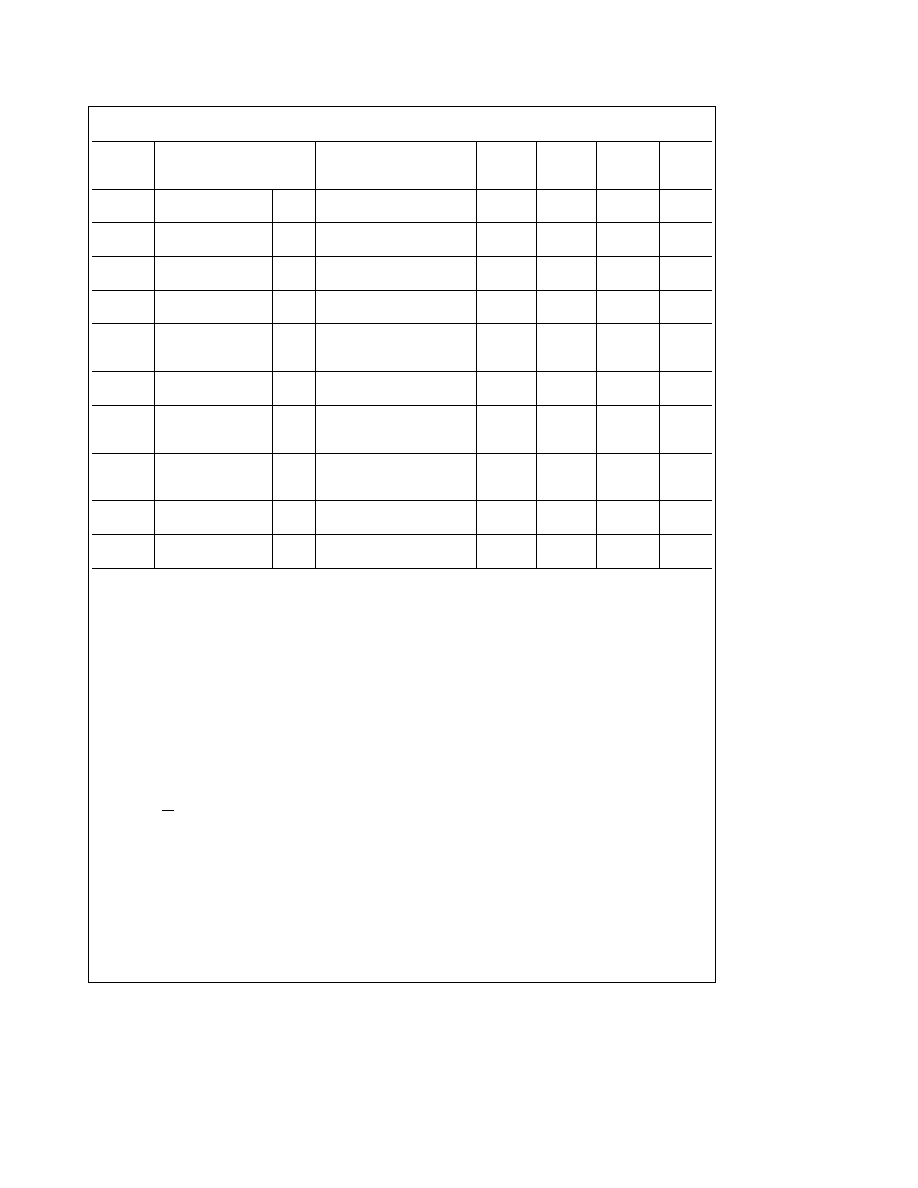
Electrical Characteristics
The following specifications apply for V
CC
e
V
a
e
5V (no V
a
on ADC0852)
V
REF
s
V
CC
a
0 1V f
CLK
e
250 kHz unless otherwise specified Boldface limits apply from T
MIN
to T
MAX
all other limits T
A
e
T
J
e
25 C
ADC0852CCN
ADC0854CCN
Parameter
Conditions
Typ
Tested
Design
Units
(Note 4)
Limit
Limit
(Note 5)
(Note 6)
CONVERTER AND MULTIPLEXER CHARACTERISTICS
Total Unadjusted
V
REF
Forced to
Error (Note 7)
5 000 V
DC
ADC0852 4 CCN
g
1
g
1
LSB
Comparator Offset
ADC0852 4 CCN
2 5
20
mV
Minimum Total Ladder
ADC0854
Resistance
(Note 15)
3 5
1 3
1 3
kX
Maximum Total Ladder
ADC0854
Resistance
(Note 15)
3 5
5 4
5 9
kX
Minimum Common-Mode
All MUX Inputs
Input (Note 8)
and COM Input
GND ≠ 0 05
GND ≠ 0 05
V
Maximum Common-Mode
All MUX Inputs
Input (Note 8)
and COM Input
V
CC
a
0 05
V
CC
a
0 05
V
DC Common-Mode Error
g
g
g
LSB
Power Supply Sensitivity
V
CC
e
5V
g
5%
g
g
g
LSB
V
Z
Internal
15 mA into V
a
diode
MIN
6 3
V
breakdown
MAX
8 5
V
at V
a
(Note 3)
I
OFF
Off Channel Leakage
On Channel
e
5V
b
1
m
A
Current (Note 9)
Off Channel
e
0V
b
200
nA
On Channel
e
0V
a
1
m
A
Off Channel
e
5V
a
200
nA
2

Electrical Characteristics
(Continued)
The following specifications apply for V
CC
e
V
a
e
5V (no V
a
on ADC0852) f
CLK
e
250 kHz unless otherwise specified
Boldface limits apply from T
MIN
to T
MAX
all other limits T
A
e
T
J
e
25 C
ADC0852CCN
ADC0854CCN
Parameter
Conditions
Typ
Tested
Design
Units
(Note 4)
Limit
Limit
(Note 5)
(Note 6)
CONVERTER AND MULTIPLEXER CHARACTERISTICS
(Continued)
I
ON
On Channel Leakage
On Channel
e
5V
a
1
m
A
Current (Note 9)
Off Channel
e
0V
a
200
nA
On Channel
e
0V
b
1
m
A
Off Channel
e
5V
b
200
nA
DIGITAL AND DC CHARACTERISTICS
V
IN(1)
Logical ``1'' Input
V
CC
e
5 25V
2 0
2 0
V
Voltage
V
IN(0)
Logical ``0'' Input
V
CC
e
4 75V
0 8
0 8
V
Voltage
I
IN(1)
Logical ``1'' Input
V
IN
e
V
CC
0 005
1
1
m
A
Current
I
IN(0)
Logical ``0'' Input
V
IN
e
0V
b
0 005
b
1
b
1
m
A
Current
V
OUT(1)
Logical ``1'' Output
V
CC
e
4 75V
Voltage
I
OUT
e b
360 mA
2 4
2 4
V
I
OUT
e b
10 mA
4 5
4 5
V
V
OUT(0)
Logical ``0'' Output
I
OUT
e
1 6 mA
Voltage
V
CC
e
4 75V
0 4
0 4
V
I
OUT
TRI-STATE Output
CS
e
Logical ``1''
Current (DO)
V
OUT
e
0 4V
b
0 1
b
3
b
3
m
A
V
OUT
e
5V
0 1
3
3
m
A
I
SOURCE
V
OUT
Short to GND
b
14
b
7 5
b
6 5
mA
I
SINK
V
OUT
Short to V
CC
16
9 0
8 0
mA
I
CC
Supply Current
Includes DAC
ADC0852
Ladder Current
2 7
6 5
6 5
mA
I
CC
Supply Current
Does not Include DAC
ADC0854 (Note 3)
Ladder Current
0 9
2 5
2 5
mA
3
AC Characteristics
t
r
e
t
f
e
20 ns T
A
e
25 C
Typ
Tested
Design
Symbol
Parameter
Conditions
(Note 4)
Limit
Limit
Units
(Note 5)
(Note 6)
f
CLK
Clock Frequency
MIN
10
kHz
(Note 12)
MAX
400
kHz
t
D1
Rising Edge of Clock
C
L
e
100 pF
650
1000
ns
to ``DO'' Enabled
t
r
Comparator Response
Not Including
2
a
1 ms
1 f
CLK
Time (Note 13)
Addressing Time
Clock Duty Cycle
MIN
40
%
(Note 10)
MAX
60
%
t
SET-UP
CS Falling Edge or
MAX
250
ns
Data Input Valid to
CLK Rising Edge
t
HOLD
Data Input Valid after
MIN
90
ns
CLK Rising Edge
t
pd1
t
pd0
CLK Falling Edge to
MAX
C
L
e
100 pF
650
1000
ns
Output Data Valid
(Note 11)
t
1H
t
0H
Rising Edge of CS to
MAX
C
L
e
10 pF R
L
e
10k
125
250
ns
Data Output Hi-Z
C
L
e
100 pF R
L
e
2k
500
500
ns
(see TRI-STATE Test Circuits)
C
IN
Capacitance of Logic
5
pF
Input
C
OUT
Capacitance of Logic
5
pF
Outputs
Note 1
Absolute Maximum Ratings indicate limits beyond which damage to the device may occur DC and AC electrical specifications do not apply when
operating the device beyond its specified operating conditions
Note 2
All voltages are measured with respect to ground
Note 3
Internal zener diodes (approx 7V) are connected from V
a
to GND and V
CC
to GND The zener at V
a
can operate as a shunt regulator and is connected
to V
CC
via a conventional diode Since the zener voltage equals the A D's breakdown voltage the diode ensures that V
CC
will be below breakdown when the
device is powered from V
a
Functionality is therefore guaranteed for V
a
operation even though the resultant voltage at V
CC
may exceed the specified Absolute
Max of 6 5V It is recommended that a resistor be used to limit the max current into V
a
Note 4
Typicals are at 25 C and represent most likely parametric norm
Note 5
Tested and guaranteed to National AOQL (Average Outgoing Quality Level)
Note 6
Guaranteed but not 100% production tested These limits are not used to calculate outgoing quality levels
Note 7
Total unadjusted error includes comparator offset DAC linearity and multiplexer error It is expressed in LSBs of the threshold DAC's input code
Note 8
For V
IN
(
b
)
t
V
IN
(
a
) the output will be 0 Two on-chip diodes are tied to each analog input (see Block Diagram) which will forward conduct for analog input
voltages one diode drop below ground or one diode drop greater than the V
CC
supply Be careful during testing at low V
CC
levels (4 5V) as high level analog inputs
(5V) can cause this input diode to conduct
especially at elevated temperatures and cause errors for analog inputs near full-scale The spec allows 50 mV forward
bias of either diode This means that as long as the analog V
IN
or V
REF
does not exceed the supply voltage by more than 50 mV the output code will be correct To
achieve an absolute 0 V
DC
to 5 V
DC
input voltage range will therefore require a minimum supply voltage of 4 950 V
DC
over temperature variations initial tolerance
and loading
Note 9
Leakage current is measured with the clock not switching
Note 10
A 40% to 60% clock duty cycle range ensures proper operation at all clock frequencies In the case that an available clock has a duty cycle outside of
these limits then 1 6 mS
s
CLK Low
s
60 mS and 1 6 mS
s
CLK HIGH
s
%
Note 11
With CS low and programming complete D0 is updated on each falling CLK edge However each new output is based on the comparison completed 0 5
clock cycles prior (see
Figure 5 )
Note 12
Error specs are not guaranteed at 400 kHz (see graph Comparator Error vs f
CLK
)
Note 13
See text section 1 2
Note 14
Human body model 100 pF discharged through a 1 5 kX resistor
Note 15
Because the reference ladder of the ADC0852 is internally connected to V
CC
ladder resistance cannot be directly tested for the ADC0852 Ladder
current is included in the ADC0852's supply current specification
4
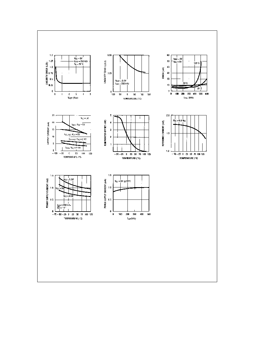
Typical Performance Characteristics
Internal DAC Linearity
Error vs V
REF
Voltage
Internal DAC Linearity
Error vs Temperature
Comparator Error vs f
CLK
Output Current vs
Temperature
Comparator Offset vs
Temperature
I
REF
Reference
Current vs Temp ADC0854
I
CC
Power Supply Current
vs Temperature ADC0854
I
CC
Power Supply
Current vs f
CLK
ADC0854
TL H 5521 ≠ 2
For ADC0852 add I
REF
5