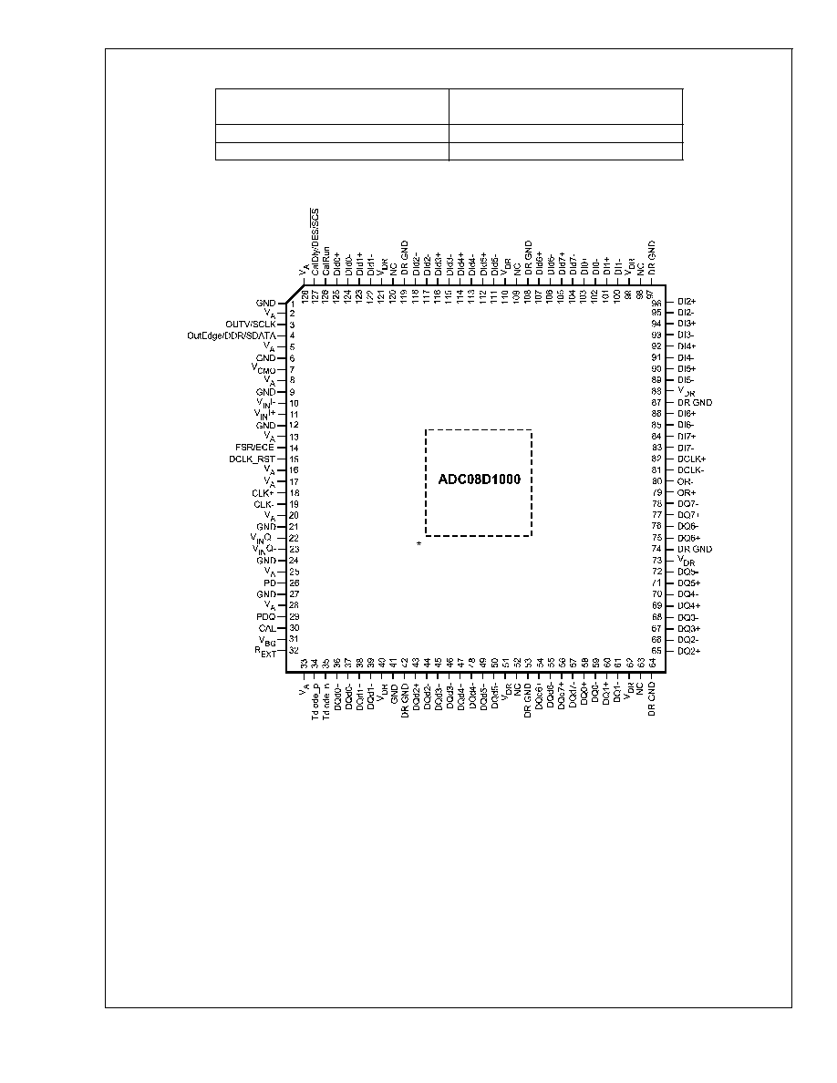
ADC08D1000
High Performance, Low Power, Dual 8-Bit, 1 GSPS A/D
Converter
General Description
NOTE: This product is currently in development. ALL
specifications are design targets and are subject to
change.
The ADC08D1000 is a dual, low power, high performance
CMOS analog-to-digital converter that digitizes signals to 8
bits resolution at sampling rates up to 1.6 GSPS. Consuming
a typical 1.6 Watts at 1 GSPS from a single 1.9 Volt supply,
this device is guaranteed to have no missing codes over the
full operating temperature range. The unique folding and
interpolating architecture, the fully differential comparator
design, the innovative design of the internal sample-and-
hold amplifier and the self-calibration scheme enable a very
flat response of all dynamic parameters beyond Nyquist,
producing a high 7.5 ENOB with a 500 MHz input signal and
a 1 GHz sample rate while providing a 10
-18
B.E.R. Output
formatting is offset binary and the LVDS digital outputs are
compliant with IEEE 1596.3-1996, with the exception of a
reduced common mode voltage of 0.8V.
Each converter has a 1:2 demultiplexer that feeds two LVDS
buses and reduces the output data rate on each bus to half
the sampling rate. The two converters can be interleaved
and used as a single 2 GSPS ADC.
The converter typically consumes less than 20 mW in the
Power Down Mode and is available in a 128-lead, thermally
enhanced exposed pad LQFP and operates over the indus-
trial (-40°C
T
A
+85°C) temperature range.
Features
n
Internal Sample-and-Hold
n
Single +1.9V
±
0.1V Operation
n
Choice of SDR or DDR output clocking
n
Interleave Mode for 2x Sampling Rate
n
Multiple ADC Synchronization Capability
n
Guaranteed No Missing Codes
n
Serial Interface for Extended Control
n
Fine Adjustment of Input Full-Scale Range and Offset
Key Specifications
n
Resolution
8 Bits
n
Max Conversion Rate
1 GSPS (min)
n
Bit Error Rate
10
-18
(typ)
n
ENOB
@
500 MHz Input
7.5 Bits (typ)
n
DNL
±
0.25 LSB (typ)
n
Power Consumption
-- Operating
1.6 W (typ)
-- Power Down Mode
20 mW (typ)
Applications
n
Direct RF Down Conversion
n
Digital Oscilloscopes
n
Satellite Set-top boxes
n
Communications Systems
n
Test Instrumentation
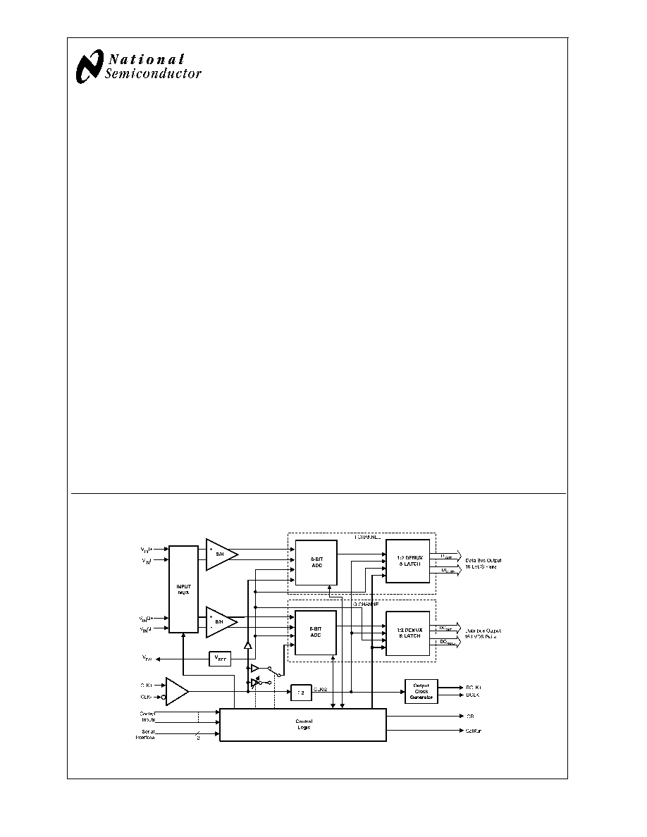
Block Diagram
20097453
ADVANCE INFORMATION
September 2004
High
Performance,
Low
Power
,
Dual
8-Bit,
1
GSPS
A/D
Converter
© 2004 National Semiconductor Corporation
DS200974
www.national.com
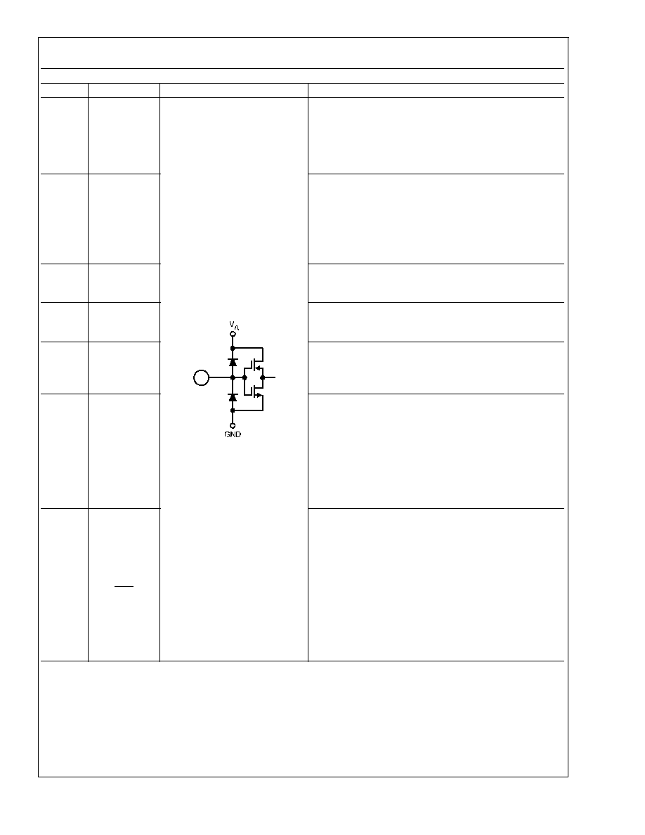
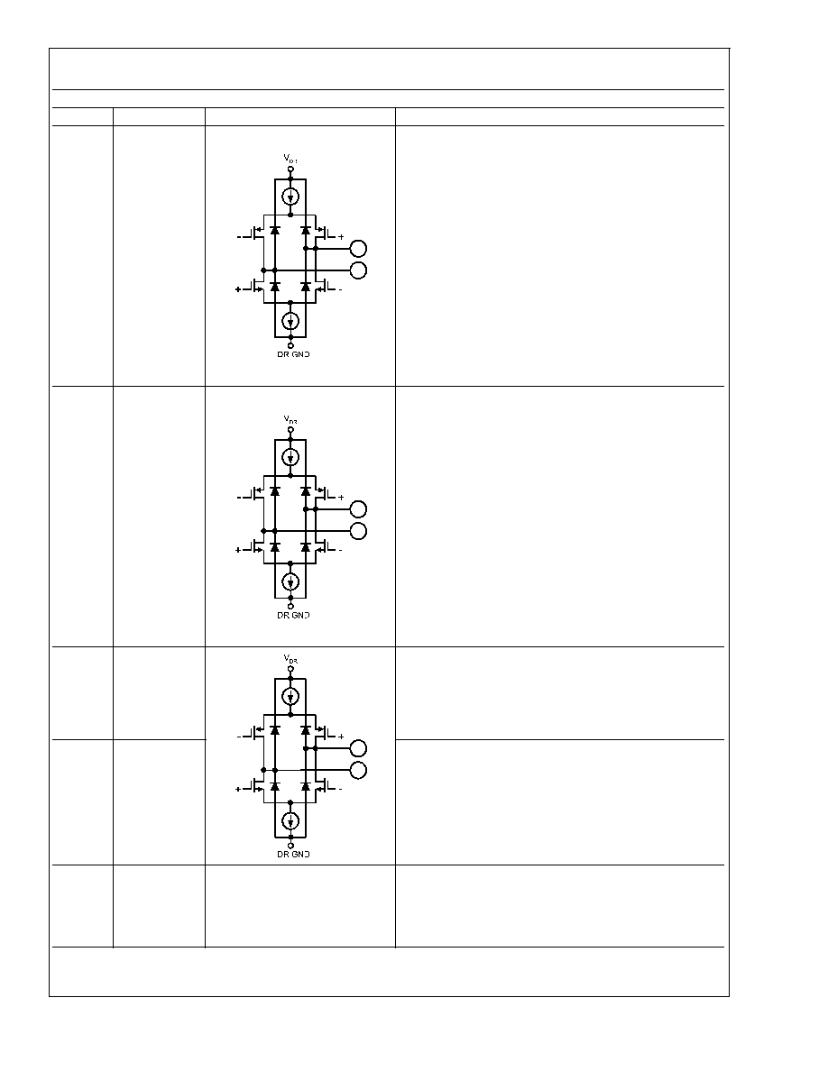
Pin Descriptions and Equivalent Circuits
Pin Functions
Pin No.
Symbol
Equivalent Circuit
Description
3
OutV / SCLK
Output Voltage Amplitude and Serial Interface Clock. Tie this
pin high for normal differential DCLK and data amplitude.
Ground this pin for a reduced differential output amplitude and
reduced power consumption. See Section 1.1.6. When the
extended control mode is enabled, this pin functions as the
SCLK input which clocks in the serial data. See Section 1.3
4
OutEdge / DDR
/ SDATA
DCLK Edge Select, Double Data Rate Enable and Serial Data
Input. This input sets the output edge of DCLK+ at which the
output data transitions. (See Section 1.1.5.2). When this pin is
floating or connected to 1/2 the supply voltage, DDR clocking
is enabled. When the extended control mode is enabled, this
pin functions as the (SDATA) input. See Section 1.2 for
details on the extended control mode.
15
DCLK_RST
DCLK Reset. A positive pulse on this pin is used to reset and
synchronize the DCLK outs of multiple converters. See
Section 1.5 for detailed description.
26
29
PD
PDQ
Power Down Pins. A logic high on the PD pin puts the entire
device into the Power Down Mode. A logic high on the PDQ
pin puts only the "Q" ADC into the Power Down mode.
30
CAL
Calibration Cycle Initiate. A minimum 10 input clock cycles
logic low followed by a minimum of 10 input clock cycles high
on this pin initiates the self calibration sequence. See Section
2.4.2.
14
FSR/ECE
Full Scale Range Select and Extended Control Enable. In
non-extended control mode, a logic low on this pin sets the
full-scale differential input range to 600 mV
P-P
. A logic high on
this pin sets the full-scale differential input range to 800
mV
P-P
. See Section 1.1.4. To enable the extended control
mode, whereby the serial interface and control registers are
employed, allow this pin to float or connect it to a voltage
equal to V
A
/2. See Section 1.2 for information on the
extended control mode.
127
CalDly / DES /
SCS
Calibration Delay, Dual Edge Sampling and Serial Interface
Chip Select. With a logic high or low on pin 14, this pin
functions as Calibration Delay and sets the number of input
clock cycles after power up before calibration begins (See
Section 1.1.1). With pin 14 floating, this pin acts as the enable
pin for the serial interface input and the CalDly value
becomes "0" (short delay with no provision for a long
power-up calibration delay). When this pin is floating or
connected to a voltage equal to V
A
/2, DES (Dual Edge
Sampling) mode is selected where the "I" input is sampled at
twice the input clock rate and the "Q" input is ignored. See
Section 1.1.5.1.
ADC08D1000
www.national.com
3
Pin Descriptions and Equivalent Circuits
(Continued)
Pin Functions
Pin No.
Symbol
Equivalent Circuit
Description
18
19
CLK+
CLK-
LVDS Clock input pins for the ADC. The differential clock
signal must be a.c. coupled to these pins. The input signal is
sampled on the falling edge of CLK+. See Section 2.3.
11
10
.
22
23
V
IN
I+
V
IN
I-
.
V
IN
Q+
V
IN
Q-
Analog signal inputs to the ADC. The differential full-scale
input range is 600 mV
P-P
when the FSR pin is low, or 800
mV
P-P
when the FSR pin is high.
7
V
CMO
Common Mode Voltage. The voltage output at this pin is
required to be the common mode input voltage at V
IN
+ and
V
IN
- when d.c. coupling is used. This pin should be grounded
when a.c. coupling is used at the analog inputs. This pin is
capable of sourcing or sinking 100µA. See Section 2.2.
31
V
BG
Bandgap output voltage capable of 100 µA source/sink.
126
CalRun
Calibration Running indication. This pin is at a logic high when
calibration is running.
32
R
EXT
External bias resistor connection. Nominal value is 3.3k-Ohms
(
±
0.1%) to ground. See Section 1.1.1.
34
35
Tdiode_P
Tdiode_N
Temperature Diode Positive (Anode) and Negative (Cathode)
for die temperature measurements. See Section 2.6.2.
ADC08D1000
www.national.com
4
Pin Descriptions and Equivalent Circuits
(Continued)
Pin Functions
Pin No.
Symbol
Equivalent Circuit
Description
83 / 78
84 / 77
85 / 76
86 / 75
89 / 72
90 / 71
91 / 70
92 / 69
93 / 68
94 / 67
95 / 66
96 / 65
100 / 61
101 / 60
102 / 59
103 / 58
DI7- / DQ7-
DI7+ / DQ7+
DI6- / DQ6-
DI6+ / DQ6+
DI5- / DQ5-
DI5+ / DQ5+
DI4- / DQ4-
DI4+ / DQ4+
DI3- / DQ3-
DI3+ / DQ3+
DI2- / DQ2-
DI2+ / DQ2+
DI1- / DQ1-
DI1+ / DQ1+
DI0- / DQ0-
DI0+ / DQ0+
I and Q channel LVDS Data Outputs that are not delayed in
the output demultiplexer. Compared with the DId and DQd
outputs, these outputs represent the later time samples.
These outputs should always be terminated with a 100
differential resistor.
104 / 57
105 / 56
106 / 55
107 / 54
111 / 50
112 / 49
113 / 48
114 / 47
115 / 46
116 / 45
117 / 44
118 / 43
122 / 39
123 / 38
124 / 37
125 / 36
DId7- / DQd7-
DId7+ / DQd7+
DId6- / DQd6-
DId6+ / DQd6+
DId5- / DQd5-
DId5+ / DQd5+
DId4- / DQd4-
DId4+ / DQd4+
DId3- / DQd3-
DId3+ / DQd3+
DId2- / DQd2-
DId2+ / DQd2+
DId1- / DQd1-
DId1+ / DQd1+
DId0- / DQd0-
DId0+ / DQd0+
I and Q channel LVDS Data Outputs that are delayed by one
CLK cycle in the output demultiplexer. Compared with the
DI/DQ outputs, these outputs represent the earlier time
sample. These outputs should always be terminated with a
100
differential resistor.
79
80
OR+
OR-
Out Of Range output. A differential high at these pins
indicates that the differential input is out of range (outside the
range
±
300 mV or
±
400 mV as defined by the FSR pin).
82
81
DCLK+
DCLK-
Differential Clock outputs used to latch the output data.
Delayed and non-delayed data outputs are supplied
synchronous to this signal. This signal is at 1/2 the input clock
rate in SDR mode and at 1/4 the input clock rate in the DDR
mode.
2, 5, 8,
13, 16,
17, 20,
25, 28,
33, 128
V
A
Analog power supply pins. Bypass these pins to ground.
ADC08D1000
www.national.com
5