ADC08L060
8-Bit, 10 MSPS to 60 MSPS, 0.65 mW/MSPS A/D
Converter with Internal Sample-and-Hold
General Description
The ADC08L060 is a low-power, 8-bit, monolithic analog-to-
digital converter with an on-chip track-and-hold circuit. Opti-
mized for low cost, low power, small size and ease of use,
this product operates at conversion rates of 10 MSPS to
60 MSPS while consuming just 0.65 mW per MHz of clock
frequency, or 39 mW at 60 MSPS. Raising the PD pin puts
the ADC08L060 into a Power Down mode where it con-
sumes
<
1.0 mW.
The unique architecture achieves 7.6 Effective Bits. The
ADC08L060 is resistant to latch-up and the outputs are
short-circuit proof. The top and bottom of the ADC08L060's
reference ladder are available for connections, enabling a
wide range of input possibilities. The digital outputs are
TTL/CMOS compatible with a separate output power supply
pin to support interfacing with 1.8V to 3V logic. The digital
inputs (CLK and PD) are TTL/CMOS compatible.
The ADC08L060 is offered in a 24-lead plastic package
(TSSOP) and is specified over the industrial temperature
range of -40�C to +85�C.
Features
n
Single-ended input
n
Internal sample-and-hold function
n
Low voltage (single +3V) operation
n
Small package
n
Power-down feature
Key Specifications
n
Resolution
8 bits
n
Conversion rate
60 MSPS
n
DNL
�
0.25 LSB (typ)
n
INL
+0.5/-0.2 LSB (typ)
n
SNR (10.1 MHz)
48 dB (typ)
n
ENOB (10.1 MHz)
7.6 bits (typ)
n
THD (10.1 MHz)
-57 dB (typ)
n
Latency
5 Clock Cycles
n
No missing codes
Guaranteed
n
Power Consumption
n
Operating
0.65 mW/MSPS (typ)
n
Power down
<
1.0 mW (typ)
Applications
n
Digital Imaging
n
Set-top boxes
n
Portable Instrumentation
n
Communication Systems
n
X-ray imaging
n
Viterbi decoders
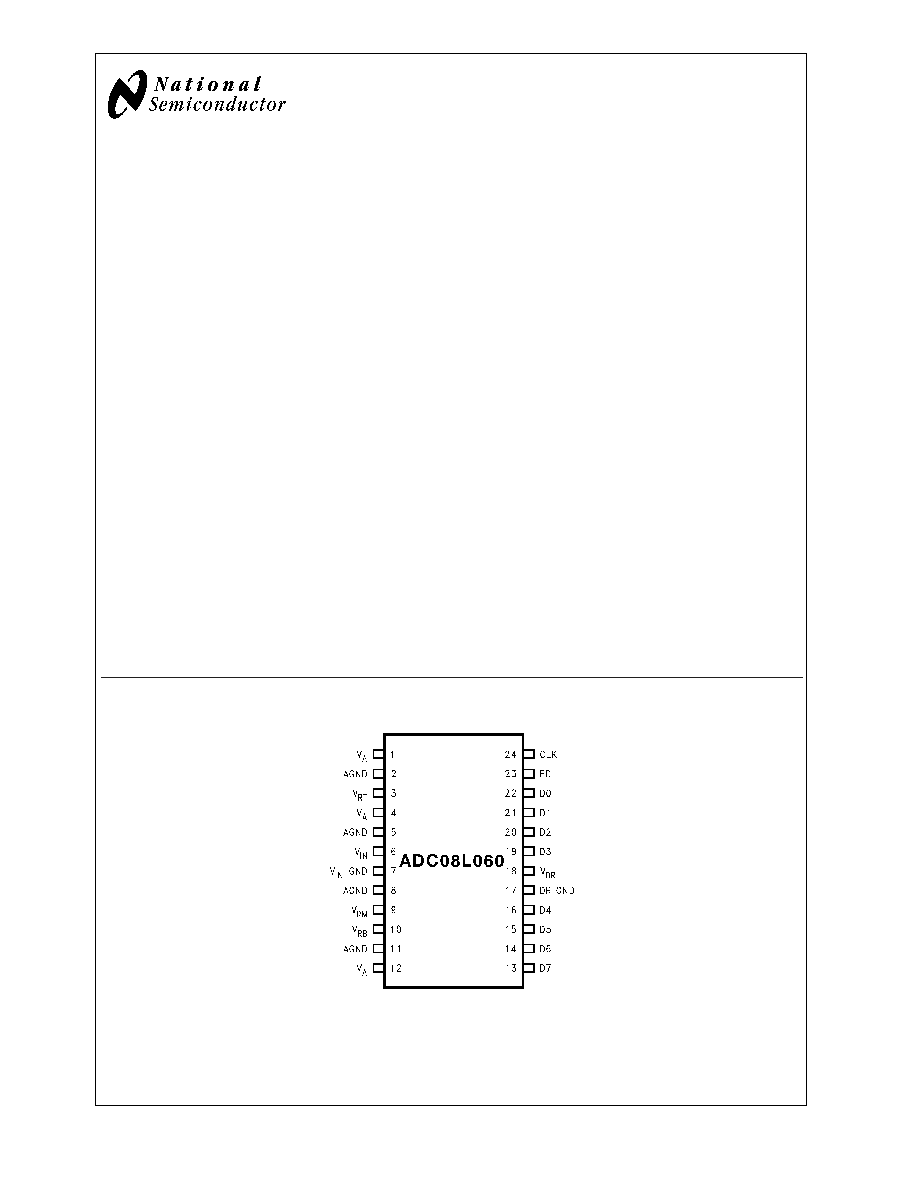
Pin Configuration
20041701
November 2002
ADC08L060
8-Bit,
10
MSPS
to
60
MSPS,
0.65
mW/MSPS
A/D
Converter
with
Internal
Sample-and-Hold
� 2002 National Semiconductor Corporation
DS200417
www.national.com
Ordering Information
ADC08L060CIMT
TSSOP
ADC08L060CIMTX
TSSOP (tape and reel)
ADC08L060EVAL
Evaluation Board
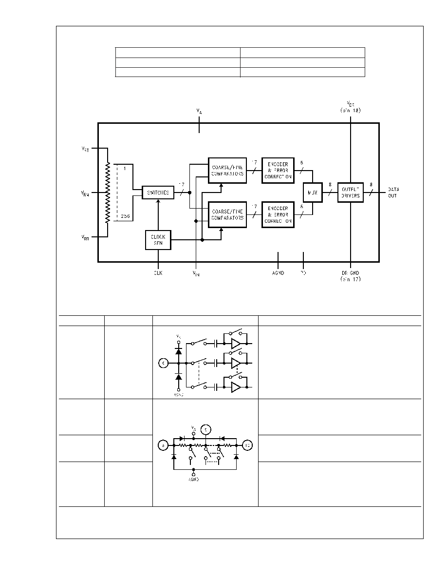
Block Diagram
20041702
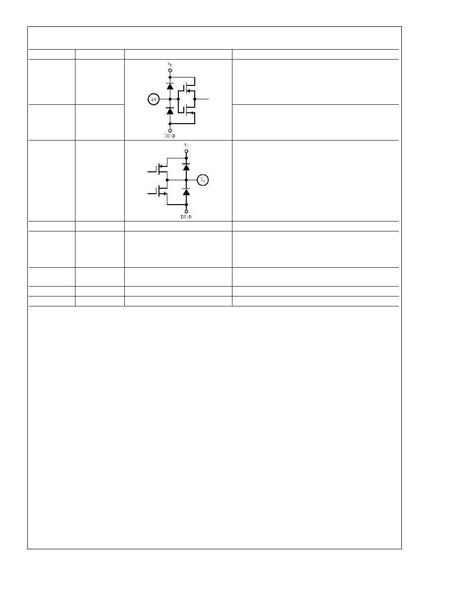
Pin Descriptions and Equivalent Circuits
Pin No.
Symbol
Equivalent Circuit
Description
6
V
IN
Analog signal input. Conversion range is V
RB
to V
RT
.
3
V
RT
Analog Input that is the high (top) side of the reference
ladder of the ADC. Nominal range is 0.5V to V
A
. Voltage
on V
RT
and V
RB
inputs define the V
IN
conversion range.
Bypass well. See Section 2.0 for more information.
9
V
RM
Mid-point of the reference ladder. This pin should be
bypassed to a quiet point in the analog ground plane with
a 0.1 �F capacitor.
10
V
RB
Analog Input that is the low side (bottom) of the
reference ladder of the ADC. Nominal range is 0.0V to
(V
RT
� 0.5V). Voltage on V
RT
and V
RB
inputs define the
V
IN
conversion range. Bypass well. See Section 2.0 for
more information.
ADC08L060
www.national.com
2
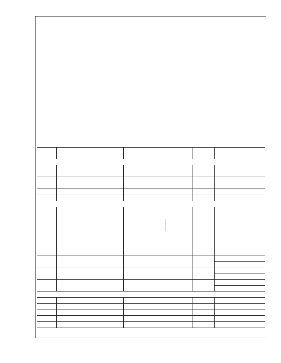
Pin Descriptions and Equivalent Circuits
(Continued)
Pin No.
Symbol
Equivalent Circuit
Description
23
PD
Power Down input. When this pin is high, the converter is
in the Power Down mode and the data output pins hold
the last conversion result.
24
CLK
CMOS/TTL compatible digital clock Input. V
IN
is sampled
on the rising edge of CLK input.
13 thru 16
and
19 thru 22
D0�D7
Conversion data digital Output pins. D0 is the LSB, D7 is
the MSB. Valid data is output after the rising edge of the
CLK input.
7
V
IN
GND
Reference ground for the single-ended analog input, V
IN
.
1, 4, 12
V
A
Positive analog supply pin. Connect to a quiet voltage
source of +3V. V
A
should be bypassed with a 0.1 �F
ceramic chip capacitor for each pin, plus one
10 �F capacitor. See Section 3.0 for more information.
18
V
DR
Power supply for the output drivers. If connected to V
A
,
decouple well from V
A
.
17
DR GND
The ground return for the output driver supply.
2, 5, 8, 11
AGND
The ground return for the analog supply.
ADC08L060
www.national.com
3
Absolute Maximum Ratings
(Notes 1,
2)
If Military/Aerospace specified devices are required,
please contact the National Semiconductor Sales Office/
Distributors for availability and specifications.
Supply Voltage (V
A
)
3.8V
Driver Supply Voltage (V
DR
)
V
A
+0.3V
Voltage on Any Input or Output Pin
-0.3V to V
A
Reference Voltage (V
RT
, V
RB
)
V
A
to AGND
CLK, PD Voltage Range
-0.05V to
(V
A
+ 0.05V)
Input Current at Any Pin (Note 3)
�
25 mA
Package Input Current (Note 3)
�
50 mA
Power Dissipation at T
A
= 25�C
See (Note 4)
ESD Susceptibility (Note 5)
Human Body Model
Machine Model
2500V
200V
Soldering Temperature, Infrared,
10 seconds (Note 6)
235�C
Storage Temperature
-65�C to +150�C
Operating Ratings
(Notes 1, 2)
Operating Temperature Range
-40�C
T
A
+85�C
Supply Voltage, V
A
+2.4V to +3.6V
Driver Supply Voltage, V
DR
+2.4V to V
A
Output Driver Voltage, V
DR
1.8V to V
A
Ground Difference |GND - DR GND|
0V to 300 mV
Upper Reference Voltage (V
RT
)
0.5V to (V
A
-0.3V)
Lower Reference Voltage (V
RB
)
0V to (V
RT
-0.5V)
V
IN
Voltage Range
V
RB
to V
RT
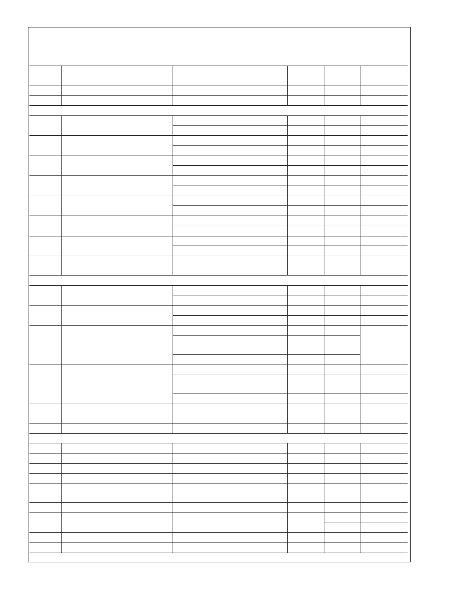
Converter Electrical Characteristics
The following specifications apply for V
A
= V
DR
= +3.0V
DC
, V
RT
= +1.9V, V
RB
= 0.3V, C
L
= 10 pF, f
CLK
= 60 MHz at 50% duty
cycle. Boldface limits apply for T
A
= T
MIN
to T
MAX
: all other limits T
A
= 25�C (Notes 7, 8)
Symbol
Parameter
Conditions
Typical
(Note 9)
Limits
(Note 9)
Units
(Limits)
DC ACCURACY
INL
Integral Non-Linearity
+0.5
-0.2
+1.9
-1.35
LSB (max)
LSB (min)
DNL
Differential Non-Linearity
�
0.25
�
0.90
LSB (max)
Missing Codes
0
(max)
FSE
Full Scale Error
3.0
�
13
mV (max)
V
OFF
Zero Scale Offset Error
19
27
mV (max)
ANALOG INPUT AND REFERENCE CHARACTERISTICS
V
IN
Input Voltage
1.6
V
RB
V (min)
V
RT
V (max)
C
IN
V
IN
Input Capacitance
V
IN
= 0.75V +0.5
Vrms
(CLK LOW)
3
pF
(CLK HIGH)
4
pF
R
IN
R
IN
Input Resistance
>
1
M
BW
Full Power Bandwidth
270
MHz
V
RT
Top Reference Voltage
1.9
V
A
V (max)
0.5
V (min)
V
RB
Bottom Reference Voltage
0.3
V
RT
- 0.5
V (max)
0
V (min)
R
REF
Reference Ladder Resistance
V
RT
to V
RB
720
590
(min)
1070
(max)
I
ref
Reference Ladder Current
VRT to VRB
2.2
1.5
mA
2.7
mA
CLK, PD DIGITAL INPUT CHARACTERISTICS
V
IH
Logical High Input Voltage
V
DR
= V
A
= 3.6V
2.0
V (min)
V
IL
Logical Low Input Voltage
V
DR
= V
A
= 2.7V
0.8
V (max)
I
IH
Logical High Input Current
V
IH
= V
DR
= V
A
= 3.6V
10
nA
I
IL
Logical Low Input Current
V
IL
= 0V, V
DR
= V
A
= 2.7V
-50
nA
C
IN
Logic Input Capacitance
3
pF
DIGITAL OUTPUT CHARACTERISTICS
ADC08L060
www.national.com
4
Converter Electrical Characteristics
(Continued)
The following specifications apply for V
A
= V
DR
= +3.0V
DC
, V
RT
= +1.9V, V
RB
= 0.3V, C
L
= 10 pF, f
CLK
= 60 MHz at 50% duty
cycle. Boldface limits apply for T
A
= T
MIN
to T
MAX
: all other limits T
A
= 25�C (Notes 7, 8)
Symbol
Parameter
Conditions
Typical
(Note 9)
Limits
(Note 9)
Units
(Limits)
V
OH
High Level Output Voltage
V
A
= V
DR
= 2.7V, I
OH
= -400 �A
2.6
2.4
V (min)
V
OL
Low Level Output Voltage
V
A
= V
DR
= 2.7V, I
OL
= 1.0 mA
0.4
0.5
V (max)
DYNAMIC PERFORMANCE
ENOB
Effective Number of Bits
f
IN
= 10.1 MHz, V
IN
= FS - 0.25 dB
7.6
6.9
Bits
f
IN
= 29 MHz, V
IN
= FS - 0.25 dB
7.4
Bits (min)
SINAD
Signal-to-Noise & Distortion
f
IN
= 10.1 MHz, V
IN
= FS - 0.25 dB
47.4
43.3
dB
f
IN
= 29 MHz, V
IN
= FS - 0.25 dB
46.1
dB (min)
SNR
Signal-to-Noise Ratio
f
IN
= 10.1 MHz, V
IN
= FS - 0.25 dB
48
44.5
dB
f
IN
= 29 MHz, V
IN
= FS - 0.25 dB
47.2
dB (min)
SFDR
Spurious Free Dynamic Range
f
IN
= 10.1 MHz, V
IN
= FS - 0.25 dB
59.1
dBc
f
IN
= 29 MHz, V
IN
= FS - 0.25 dB
54.5
dBc
THD
Total Harmonic Distortion
f
IN
= 10.1 MHz, V
IN
= FS - 0.25 dB
-56.9
dBc
f
IN
= 29 MHz, V
IN
= FS - 0.25 dB
-53.3
dBc
HD2
2nd Harmonic Distortion
f
IN
= 10.1 MHz, V
IN
= FS - 0.25 dB
-61.1
dBc
f
IN
= 29 MHz, V
IN
= FS - 0.25 dB
-54.9
dBc
HD3
3rd Harmonic Distortion
f
IN
= 10.1 MHz, V
IN
= FS - 0.25 dB
-64.2
dBc
f
IN
= 29 MHz, V
IN
= FS - 0.25 dB
-63.1
dBc
IMD
Intermodulation Distortion
f
1
= 11 MHz, V
IN
= FS - 6.25 dB
f
2
= 12 MHz, V
IN
= FS - 6.25 dB
-55
dBc
POWER SUPPLY CHARACTERISTICS
I
A
Analog Supply Current
DC Input
13
15.9
mA (max)
f
IN
= 10 MHz, V
IN
= FS - 3 dB
14
mA
DRI
D
Output Driver Supply Current
DC Input
0.04
0.2
mA (max)
f
IN
= 10 MHz, V
IN
= FS - 3 dB
4.2
mA
I
A
+
DRI
D
Total Operating Current
DC Input
13
16.1
mA (max)
f
IN
= 10 MHz, V
IN
= FS - 3 dB, PD =
Low
18.2
CLK Low, PD = Hi
0.33
PC
Power Consumption
DC Input
39
48.3
mW (max)
f
IN
= 10 MHz, V
IN
= FS - 3 dB, PD =
Low
53
mW
CLK Low, PD = Hi
0.3
mW
PSRR
1
Power Supply Rejection Ratio
FSE change with 2.7V to 3.3V change
in V
A
-51
dB
PSRR
2
Power Supply Rejection Ratio
SNR with 200 mW at 1MHz on supply
45
dB
AC ELECTRICAL CHARACTERISTICS
f
C1
Maximum Conversion Rate
80
60
MHz (min)
f
C2
Minimum Conversion Rate
10
MHz
t
CL
Minimum Clock Low Time
0.62
ns (min)
t
CH
Minimum Clock High Time
0.62
ns (min)
DC
Clock Duty Cycle
5
95
%(min)
%(max)
t
OH
Output Hold Time
CLK to Data Invalid
5.2
ns
t
OD
Output Delay
CLK to Data Transition
7.1
5.0
ns (min)
9.4
ns (max)
Pipeline Delay (Latency)
5
Clock Cycles
t
AD
Sampling (Aperture) Delay
CLK Rise to Acquisition of Data
2.6
ns
ADC08L060
www.national.com
5