
ADC1001
10-Bit µP Compatible A/D Converter
General Description
The ADC1001 is a CMOS, 10-bit successive approximation
A/D converter. The 20-pin ADC1001 is pin compatible with
the ADC0801 8-bit A/D family. The 10-bit data word is read in
two 8-bit bytes, formatted left justified and high byte first. The
six least significant bits of the second byte are set to zero, as
is proper for a 16-bit word.
Differential inputs provide low frequency input common
mode rejection and allow offsetting the analog range of the
converter. In addition, the reference input can be adjusted
enabling the conversion of reduced analog ranges with
10-bit resolution.
Key Specifications
n
Resolution
10 bits
n
Linearity error
±
1 LSB
n
Conversion time
200µS
Features
n
ADC1001 is pin compatible with ADC0801 series 8-bit
A/D converters
n
Compatible with NSC800 and 8080 µP derivatives -- no
interfacing logic needed
n
Easily interfaced to 6800 µP derivatives
n
Differential analog voltage inputs
n
Logic inputs and outputs meet both MOS and TTL
voltage level specifications
n
Works with 2.5V (LM336) voltage reference
n
On-chip clock generator
n
0V to 5V analog input voltage range with single 5V
supply
n
Operates ratiometrically or with 5 V
DC
, 2.5 V
DC
, or
analog span adjusted voltage reference
n
0.3" standard width 20-pin DIP package
Connection Diagram
Ordering Information
Temperature
Range
0∞C to +70∞C
-40∞C to +85∞C
Order Number
ADC1001CCJ-1
ADC1001CCJ
Package Outline
J20A
J20A
TRI-STATE
Æ
is a registered trademark of National Semiconductor Corp.
ADC1001
Dual-In-Line Package
DS005675-11
Top View
June 1999
ADC1001
10-Bit
µP
Compatible
A/D
Converter
© 1999 National Semiconductor Corporation
DS005675
www.national.com

Absolute Maximum Ratings
(Notes 1, 2)
If Military/Aerospace specified devices are required,
please contact the National Semiconductor Sales Office/
Distributors for availability and specifications.
Supply Voltage (V
CC
) (Note 3)
6.5V
Logic Control Inputs
-0.3V to +18V
Voltage at Other Inputs and Outputs
-0.3V to (V
CC
+0.3V)
Storage Temperature Range
-65∞C to +150∞C
Package Dissipation at T
A
=25∞C
875 mW
Lead Temp. (Soldering, 10 seconds)
300∞C
ESD Susceptibility (Note 10)
800V
Operating Conditions
(Notes 1, 2)
Temperature Range
T
MIN
T
A
T
MAX
ADC1001CCJ
-40∞C
T
A
+85∞C
ADC1001CCJ-1
0∞C
T
A
+70∞C
Range of V
CC
4.5 V
DC
to 6.3 V
DC
Converter Characteristics
Converter Specifications: V
CC
=5 V
DC
, V
REF
/2=2.500 V
DC
, T
MIN
T
A
T
MAX
and f
CLK
=410 kHz unless otherwise specified.
Parameter
Conditions
MIn
Typ
Max
Units
Linearity Error
±
1
LSB
Zero Error
±
2
LSB
Full-Scale Error
±
2
LSB
Total Ladder Resistance (Note 9)
Input Resistance at Pin 9
2.2
4.8
K
Analog Input Voltage Range
(Note 4) V(+) or V(-)
GND-0.05
V
CC
+0.05
V
DC
DC Common-Mode Error
Over Analog Input Voltage Range
±
1
/
8
LSB
Power Supply Sensitivity
V
CC
=5 V
DC
±
5% Over
±
1
/
8
LSB
Allowed V
IN
(+) and V
IN
(-)
Voltage Range (Note 4)
AC Electrical Characteristics
Timing Specifications: V
CC
=5 V
DC
and T
A
=25∞C unless otherwise specified.
Symbol
Parameter
Conditions
MIn
Typ
Max
Units
T
c
Conversion Time
(Note 5)
80
90
1/f
CLK
f
CLK
=410 kHz
195
220
µs
f
CLK
Clock Frequency
(Note 8)
100
1260
kHz
Clock Duty Cycle
40
60
%
CR
Conversion Rate In Free-Running
INTR tied to WR with
4600
conv/s
Mode
CS =0 V
DC
, f
CLK
=410 kHz
t
W(WR)L
Width of WR Input (Start Pulse
CS =0 V
DC
(Note 6)
150
ns
Width)
t
ACC
Access Time (Delay from
C
L
=100 pF
170
300
ns
Falling Edge of RD to Output
Data Valid)
t
1H
, t
0H
TRI-STATE
Æ
Control (Delay
C
L
=10 pF, R
L
=10k
125
200
ns
from Rising Edge of RD to
(See TRI-STATE Test
Hi-Z State)
Circuits)
t
WI
, t
RI
Delay from Falling Edge
300
450
ns
of WR or RD to Reset of INTR
t
1rs
INTR to 1st Read Set-Up Time
550
400
ns
C
IN
Input Capacitance of Logic
5
7.5
pF
Control Inputs
C
OUT
TRI-STATE Output
5
7.5
pF
Capacitance (Data Buffers)
www.national.com
2

DC Electrical Characteristics
The following specifications apply for V
CC
=5 V
DC
and T
MIN
T
A
T
MAX
, unless otherwise specified.
Symbol
Parameter
Conditions
MIn
Typ
Max
Units
CONTROL INPUTS [Note: CLK IN is the input of a Schmitt trigger circuit and is therefore specified separately]
V
IN
(1)
Logical "1" Input Voltage
V
CC
=5.25 V
DC
2.0
15
V
DC
(Except CLK IN)
V
IN
(0)
Logical "0" Input Voltage
V
CC
=4.75 V
DC
0.8
V
DC
(Except CLK IN)
I
IN
(1)
Logical "1" Input Current
V
IN
=5 V
DC
0.005
1
µA
DC
(All Inputs)
I
IN
(0)
Logical "0" input Current
V
IN
=0 V
DC
-1
-0.005
µA
DC
(All Inputs)
CLOCK IN
V
T
+
CLK IN Positive Going
2.7
3.1
3.5
V
DC
Threshold Voltage
V
T
-
CLK IN Negative Going
1.5
1.8
2.1
V
DC
Threshold Voltage
V
H
CLK IN Hysteresis
0.6
1.3
2.0
V
DC
(V
T
+)-(V
T
-)
OUTPUTS AND INTR
V
OUT
(0)
Logical "0" Output Voltage
I
OUT
=1.6 mA, V
CC
=4.75 V
DC
0.4
V
DC
V
OUT
(1)
Logical "1" Output Voltage
I
O
=-360 µA, V
CC
=4.75 V
DC
2.4
V
DC
I
O
=-10 µA, V
CC
=4.75 V
DC
4.5
V
DC
I
OUT
TRI-STATE Disabled Output
V
OUT
=0.4 V
DC
0.1
-100
µA
DC
Leakage (All Data Buffers)
V
OUT
=5 V
DC
0.1
3
µA
DC
I
SOURCE
V
OUT
Short to GND, T
A
=25∞C
4.5
6
mA
DC
I
SINK
V
OUT
Short to V
CC
, T
A
=25∞C
9.0
16
mA
DC
POWER SUPPLY
I
CC
Supply Current (Includes
f
CLK
=410 kHz,
Ladder Current)
V
REF
/2=NC, T
A
=25∞C
and CS =1
2.5
5.0
mA
Note 1: Absolute Maximum Ratings indicate limits beyond which damage to the device may occur. DC and AC electrical specifications do not apply when operating
the device beyond its specified operating conditions.
Note 2: All voltages are measured with respect to GND, unless otherwise specified. The separate A GND point should always be wired to the D GND.
Note 3: A zener diode exists, internally, from V
CC
to GND and has a typical breakdown voltage of 7 V
DC
.
Note 4: For V
IN
(-)
V
IN
(+) the digital output code will be all zeros. Two on-chip diodes are tied to each analog input (see Block Diagram) which will forward conduct
for analog input voltages one diode drop below ground or one diode drop greater than the V
CC
supply. Be careful, during testing at low V
CC
levels (4.5V), as high
level analog inputs (5V) can cause this input diode to conduct -- especially at elevated temperatures, and cause errors for analog inputs near fullscale. The spec al-
lows 50 mV forward bias of either diode. This means that as long as the analog V
IN
does not exceed the supply voltage by more than 50 mV, the output code will
be correct. To achieve an absolute 0 V
DC
to 5 V
DC
input voltage range will therefore require a minimum supply voltage of 4.950 V
DC
over temperature variations, initial
tolerance and loading.
Note 5: With an asynchronous start pulse, up to 8 clock periods may be required before the internal clock phases are proper to start the conversion process. The
start request is internally latched, see
Figure 3 .
Note 6: The CS input is assumed to bracket the WR strobe input and therefore timing is dependent on the WR pulse width. An arbitrarily wide pulse width will hold
the converter in a reset mode and the start of conversion is initiated by the low to high transition of the WR pulse (see Timing Diagrams).
Note 7: All typical values are for T
A
=25∞C.
Note 8: Accuracy is guaranteed at f
CLK
=410 kHz. At higher clock frequencies accuracy can degrade.
Note 9: The V
REF/2
pin is the center point of a two resistor divider (each resistor is 2.4k
) connected from V
CC
to ground. Total ladder input resistance is the sum
of these two equal resistors.
Note 10: Human body model, 100 pF discharged through a 1.5 k
resistor.
www.national.com
3

Typical Performance Characteristics
TRI-STATE Test Circuits and Waveforms
Logic Input Threshold
Voltage vs Supply Voltage
DS005675-14
Delay From Falling Edge of
RD to Output Data Valid
vs Load Capacitance
DS005675-15
CLK IN Schmitt Trip Levels
vs Supply Voltage
DS005675-16
Output Current vs
Temperature
DS005675-17
DS005675-3
t
1H
, C
L
=10 pF
DS005675-4
t
r
=20 ns
DS005675-5
t
0H
, C
L
=10 pF
DS005675-6
t
r
=20 ns
www.national.com
4
TRI-STATE Test Circuits and Waveforms
(Continued)
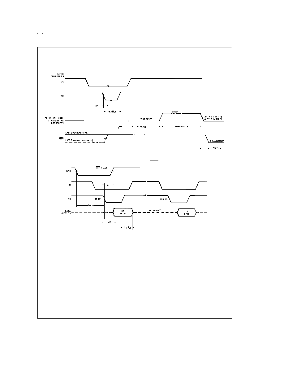
Timing Diagrams
DS005675-7
Output Enable and Reset INTR
DS005675-8
*All timing is measured from the 50% voltage points.
www.national.com
5