Äîêóìåíòàöèÿ è îïèñàíèÿ www.docs.chipfind.ru
ADC10040
10-Bit, 40 MSPS, 3V, 55.5 mW A/D Converter
General Description
The ADC10040 is a monolithic CMOS analog-to-digital con-
verter capable of converting analog input signals into 10-bit
digital words at 40 Megasamples per second (MSPS). This
converter uses a differential, pipeline architecture with digital
error correction and an on-chip sample-and-hold circuit to
provide a complete conversion solution, and to minimize
power consumption, while providing excellent dynamic per-
formance. A unique sample-and-hold stage yields a full-
power bandwidth of 400 MHz. Operating on a single 3.0V
power supply, this device consumes just 55.5 mW at
40 MSPS, including the reference current. The Standby
feature reduces power consumption to just 13.5 mW.
The differential inputs provide a full scale selectable input
swing of 2.0 V
P-P
, 1.5 V
P-P
, 1.0 V
P-P
, with the possibility of a
single-ended input. Full use of the differential input is recom-
mended for optimum performance. An internal +1.2V preci-
sion bandgap reference is used to set the ADC full-scale
range, and also allows the user to supply a buffered refer-
enced voltage for those applications requiring increased ac-
curacy. The output data format is 10-bit offset binary, or two's
complement.
This device is available in the 28-lead TSSOP package and
will operate over the industrial temperature range of -40°C to
+85°C.
Features
n
Single +3.0V operation
n
Selectable 2.0 V
P-P
, 1.5 V
P-P
, or 1.0 V
P-P
full-scale input
swing
n
400 MHz -3 dB input bandwidth
n
Low power consumption
n
Standby mode
n
On-chip reference and sample-and-hold amplifier
n
Offset binary or two's complement data format
n
Separate adjustable output driver supply to
accommodate 2.5V and 3.3V logic families
n
28-pin TSSOP package
Key Specifications
n
Resolution
10 Bits
n
Conversion Rate
40 MSPS
n
Full Power Bandwidth
400 MHz
n
DNL
±
0.3 LSB (typ)
n
SNR (f
IN
= 11 MHz)
59.6 dB (typ)
n
SFDR (f
IN
= 11 MHz)
-80 dB (typ)
n
Data Latency
6 Clock Cycles
n
Supply Voltage
+3.0V
n
Power Consumption, 40 MHz
55.5 mW
Applications
n
Ultrasound and Imaging
n
Instrumentation
n
Cellular Based Stations/Communications Receivers
n
Sonar/Radar
n
xDSL
n
Wireless Local Loops
n
Data Acquisition Systems
n
DSP Front Ends
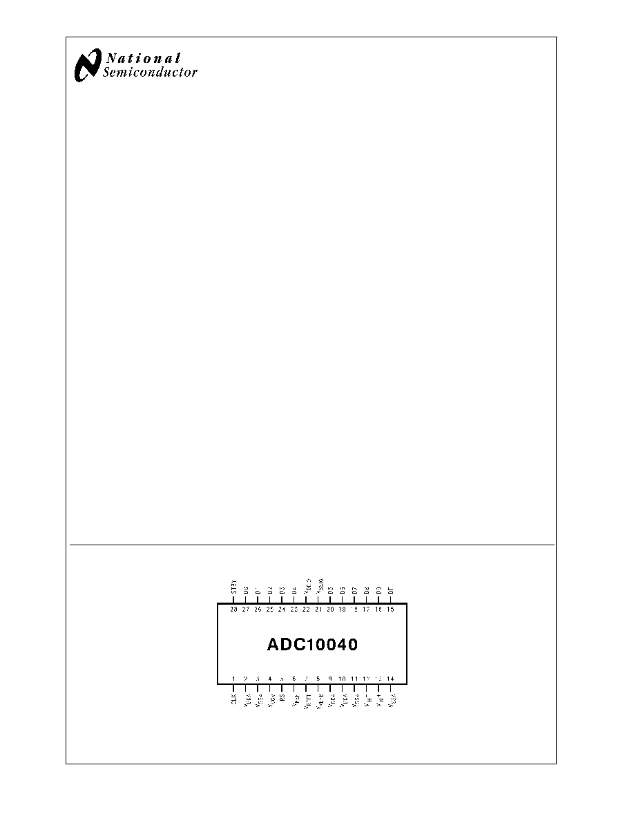
Connection Diagram
20077801
November 2004
ADC10040
10-Bit
40
MSPS
3V
,
5
5
m
W
A/D
Converter
© 2004 National Semiconductor Corporation
DS200778
www.national.com
Ordering Information
Industrial (-40°C
T
A
+85°C)
NS Package
ADC10040CIMT
28 Pin TSSOP
ADC10040CIMTX
28 Pin TSSOP Tape & Reel
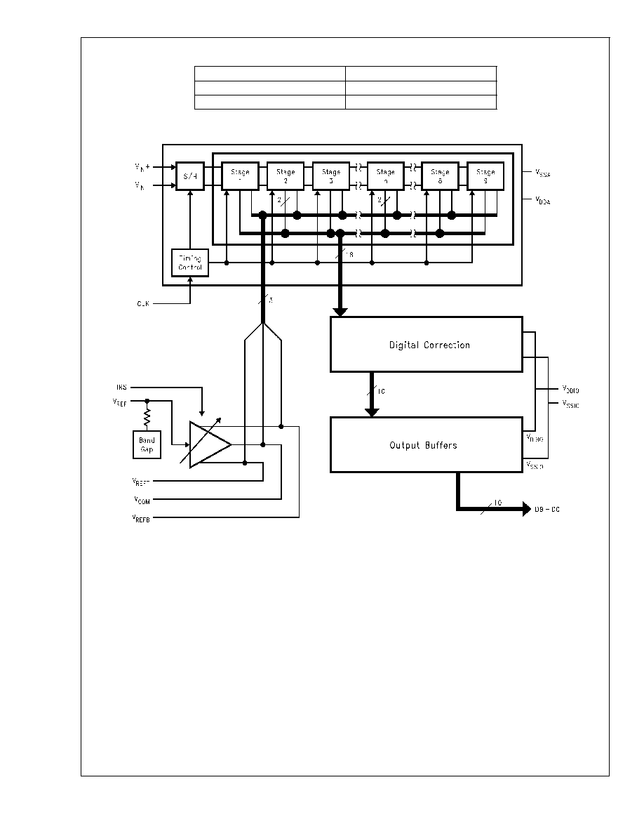
Block Diagram
20077802
ADC10040
www.national.com
2
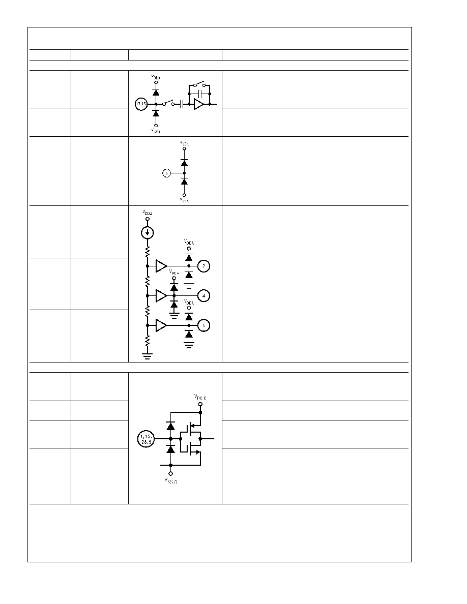
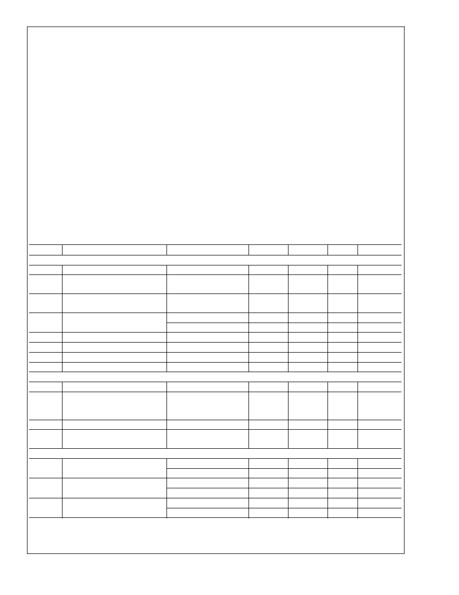
Pin Descriptions and Equivalent Circuits
Pin No.
Symbol
Equivalent Circuit
Description
ANALOG I/O
12
V
IN-
Inverting analog input signal. With a 1.2V reference the
full-scale input signal level is 1.0 V
P-P
. This pin may be tied to
V
COM
(pin 4) for single-ended operation.
13
V
IN+
Non-inverting analog input signal. With a 1.2V reference the
full-scale input signal level is 1.0 V
P-P
.
6
V
REF
Reference input. This pin should be bypassed to V
SSA
with a
0.1 µF monolithic capacitor. V
REF
is 1.20V nominal. This pin
may be driven by a 1.20V external reference if desired. Do
not load this pin.
7
V
REFT
V
REFT
and V
REFB
are high impedance reference bypass pins
only. Connect a 0.1 µF capacitor from each of these pins to
V
SSA
. These pins should not be loaded. V
COM
should also be
bypassed with a 0.1 µF capacitor to V
SSA
. V
COM
may be used
to set the input common voltage V
CM
.
4
V
COM
8
V
REFB
DIGITAL I/O
1
CLK
Digital clock input. The range of frequencies for this input is
20 MHz to 40 MHz. The input is sampled on the rising edge
of this input.
15
DF
DF = "1" Two's Complement
DF = "0" Offset Binary
28
STBY
This is the standby pin. When high, this pin sets the converter
into standby mode. When this pin is low, the converter is in
active mode.
5
IRS (Input Range
Select)
IRS = "V
DDA
" 2.0 V
P-P
input range
IRS = "V
SSA
" 1.5 V
P-P
input range
IRS = "Floating" 1.0 V
P-P
input range
If using both V
IN
+ and V
IN
- pins, (or differential mode), then
the peak-to-peak voltage refers to the differential voltage
(V
IN
+ - V
IN
-).
ADC10040
www.national.com
3
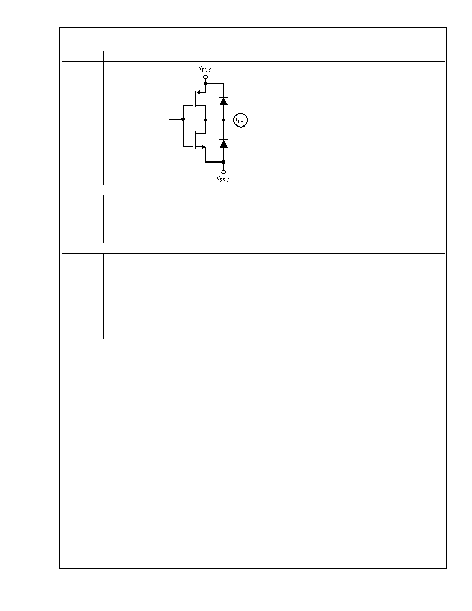
Pin Descriptions and Equivalent Circuits
(Continued)
Pin No.
Symbol
Equivalent Circuit
Description
1620,
2327
D0D9
Digital output data. D0 is the LSB and D9 is the MSB of the
binary output word.
ANALOG POWER
2, 9, 10
V
DDA
Positive analog supply pins. These pins should be connected
to a quiet 3,0V source and bypassed to analog ground with a
0.1 µF monolithic capacitor located within 1 cm of these pins.
A 4.7 µF capacitor should also be used in parallel.
3, 11, 14
V
SSA
Ground return for the analog supply.
DIGITAL POWER
22
V
DDIO
Positive digital supply pins for the ADC10040's output drivers.
This pin should be bypassed to digital ground with a 0.1 µF
monolithic capacitor located within 1 cm of this pin. A 4.7 µF
capacitor should also be used in parallel. The voltage on this
pin should never exceed the voltage on V
DDA
by more than
300 mV.
21
V
SSIO
The ground return for the digital supply for the output drivers.
This pin should be connected to the digital ground, but not
near the analog ground.
ADC10040
www.national.com
4
Absolute Maximum Ratings
(Notes 1,
2)
If Military/Aerospace specified devices are required,
please contact the National Semiconductor Sales Office/
Distributors for availability and specifications.
V
DDA
, V
DDIO
3.9V
Voltage on Any Pin to GND
-0.3V to V
DDA
or
V
DDIO
+0.3V
Input Current on Any Pin
±
25 mA
Package Input Current (Note 3)
±
50 mA
Package Dissipation at T = 25°C
See (Note 4)
ESD Susceptibility
Human Body Model (Note 5)
2500V
Machine Model (Note 5)
250V
Soldering Temperature
Infrared, 10 sec. (Note 6)
235°C
Storage Temperature
-65°C to +150°C
Operating Ratings
Operating Temperature Range
-40°C
T
A
+85°C
V
DDA
(Supply Voltage)
+2.7V to +3.6V
V
DDIO
(Output Driver Supply
Voltage)
+2.5V to V
DDA
V
REF
1.20V
|V
SSA
V
SSIO
|
100 mV
NOTE: Absolute maximum ratings are limiting values, to be applied individu-
ally, and beyond which the serviceability of the circuit may be impaired.
Functional operability under any of these conditions is not necessarily im-
plied. Exposure to maximum ratings for extended periods may affect device
reliability.
Converter Electrical Characteristics
Unless otherwise specified, the following specifications apply for V
SSA
= V
SSIO
= 0V, V
DDA
= +3.0V, V
DDIO
= +2.5V,
V
IN
= 2 V
P-P
, STBY = 0V, V
REF
= 1.20V, (External Supply) f
CLK
= 40 MHz, 50% Duty Cycle, C
L
= 10 pF/pin. Boldface limits
apply for T
A
= T
MIN
to T
MAX
: all other limits T
A
= 25°C.
Symbol
Parameter
Conditions
Min
Typ
Max
Units
STATIC CONVERTER CHARACTERISTICS
No Missing Codes Guaranteed
10
Bits
INL
Integral Non-Linearity (Note 11)
F
IN
= 250 kHz, -0 dB Full
Scale
-1.0
±
0.3
+1.0
LSB
DNL
Differential Non-Linearity
F
IN
= 250 kHz, -0 dB Full
Scale
-0.9
±
0.3
+0.9
LSB
GE
Gain Error
Positive Error
-1.5
+0.4
+1.9
% FS
Negative Error
-1.5
-0.01
+1.9
% FS
OE
Offset Error (V
IN
+ = V
IN
-)
-1.4
0.12
+1.6
% FS
Under Range Output Code
0
Over Range Output Code
1023
FPBW
Full Power Bandwidth
400
MHz
REFERENCE AND INPUT CHARACTERISTICS
V
CM
Common Mode Input Voltage
0.5
1.5
V
V
COM
Output Voltage for use as an
input common mode voltage
(Note 16)
1.45
V
V
REF
Reference Voltage
1.2
V
V
REFTC
Reference Voltage Temperature
Coefficient
±
80
ppm/°C
POWER SUPPLY CHARACTERISTICS
I
VDDA
Analog Supply Current
STBY = 1
4.5
6.0
mA
STBY = 0
18
25
mA
I
VDDIO
Digital Supply Current
STBY = 1, f
IN
= 0 Hz
0
mA
STBY = 0, f
IN
= 0 Hz
0.6
0.8
mA
PWR
Power Consumption
STBY = 1
13.5
18
mW
STBY = 0
55.5
77
mW
ADC10040
www.national.com
5
Document Outline