
ADC10154/ADC10158
10-Bit Plus Sign 4 µs ADCs with 4- or 8-Channel MUX,
Track/Hold and Reference
General Description
The ADC10154 and ADC10158 are CMOS 10-bit plus sign
successive approximation A/D converters with versatile ana-
log input multiplexers, track/hold function and a 2.5V
band-gap reference. The 4-channel or 8-channel multiplex-
ers can be software configured for single-ended, differential
or pseudo-differential modes of operation.
The input track/hold is implemented using a capacitive array
and sampled-data comparator.
Resolution can be programmed to be 8-bit, 8-bit plus sign,
10-bit or 10-bit plus sign. Lower-resolution conversions can
be performed faster.
The variable resolution output data word is read in two bytes,
and can be formatted left justified or right justified, high byte
first.
Applications
n
Process control
n
Instrumentation
n
Test equipment
Features
n
4- or 8- channel configurable multiplexer
n
Analog input track/hold function
n
0V to 5V analog input range with single +5V power
supply
n
-5V to +5V analog input voltage range with
±
5V
supplies
n
Fully tested in unipolar (single +5V supply) and bipolar
(dual
±
5V supplies) operation
n
Programmable resolution/speed and output data format
n
Ratiometric or Absolute voltage reference operation
n
No zero or full scale adjustment required
n
No missing codes over temperature
n
Easy microprocessor interface
Key Specifications
n
Resolution
10-bit plus sign
n
Integral linearity error
±
1 LSB (max)
n
Unipolar power dissipation
33 mW (max)
n
Conversion time (10-bit + sign)
4.4 µs (max)
n
Conversion time (8-bit)
3.2 µs (max)
n
Sampling rate (10-bit + sign)
166 kHz
n
Sampling rate (8-bit)
207 kHz
n
Band-gap reference
2.5V
±
2.0% (max)
ADC10158 Simplified Block Diagram
DS011225-1
November 1999
ADC10154/ADC10158
10-Bit
Plus
Sign
4
µ
s
ADCs
with
4-
or
8-Channel
MUX,
T
rack/Hold
and
Reference
© 2001 National Semiconductor Corporation
DS011225
www.national.com
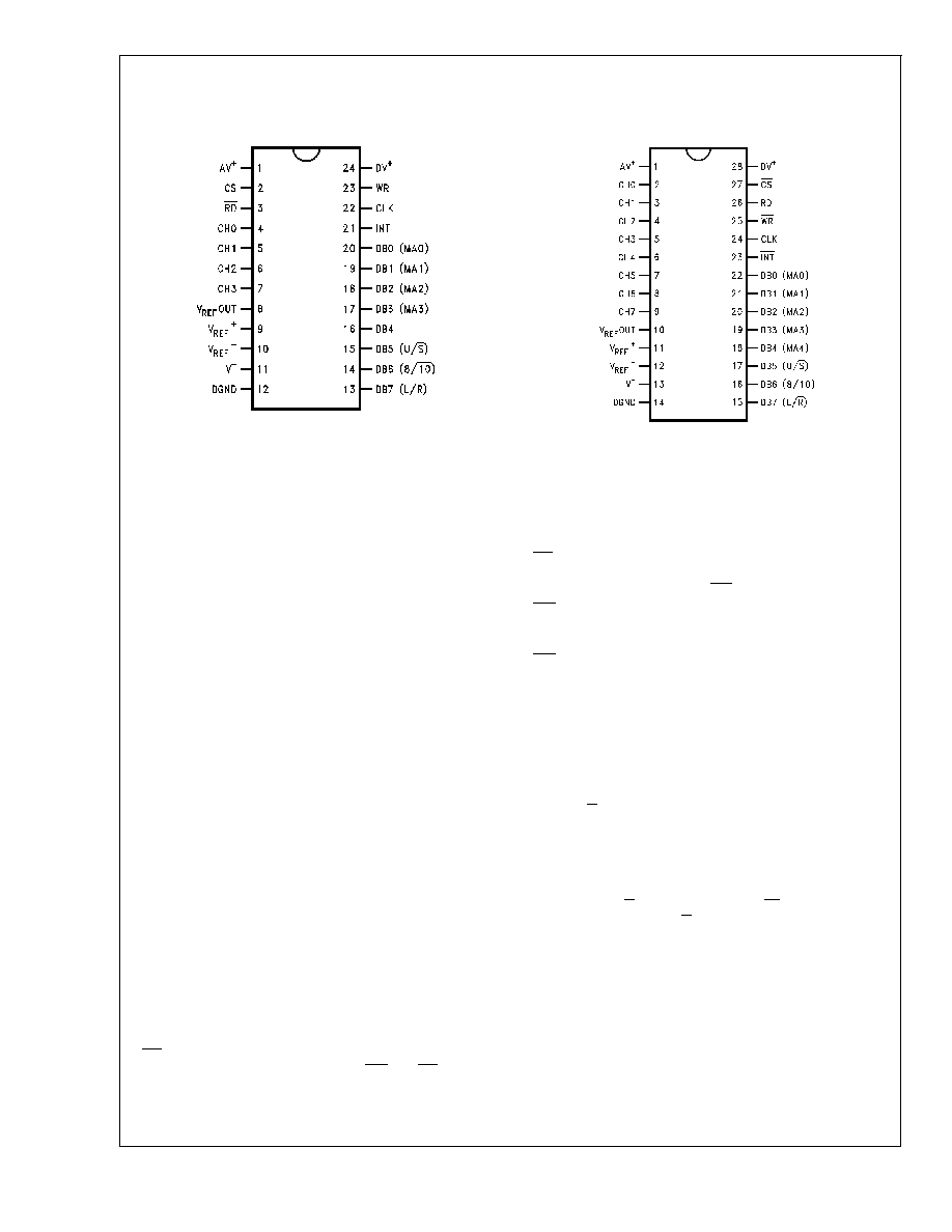
Connection Diagrams
Pin Descriptions
AV
+
This is the positive analog supply. This pin
should be bypassed with a 0.1 µF ceramic ca-
pacitor and a 10 µF tantalum capacitor to the
system analog ground.
DV
+
This is the positive digital supply. This supply
pin also needs to be bypassed with 0.1 µF
ceramic and 10 µF tantalum capacitors to the
system digital ground. AV
+
and DV
+
should be
bypassed separately and tied to same power
supply.
DGND
This is the digital ground. All logic levels are
referred to this ground.
V
-
This is the negative analog supply. For unipolar
operation this pin may be tied to the system
analog ground or to a negative supply source.
It should not go above DGND by more than
50 mV. When bipolar operation is required, the
voltage on this pin will limit the analog input's
negative voltage level. In bipolar operation this
supply pin needs to be bypassed with 0.1 µF
ceramic and 10 µF tantalum capacitors to the
system analog ground.
V
REF
+
,
V
REF
-
These are the positive and negative reference
inputs. The voltage difference between V
REF
+
and V
REF
-
will set the analog input voltage
span.
V
REF
Out
This is the internal band-gap voltage reference
output. For proper operation of the voltage ref-
erence, this pin needs to be bypassed with a
330 µF tantalum or electrolytic capacitor.
CS
This is the chip select input. When a logic low
is applied to this pin the WR and RD pins are
enabled.
RD
This is the read control input. When a logic low
is applied to this pin the digital outputs are
enabled and the INT output is reset high.
WR
This is the write control input. The rising edge
of the signal applied to this pin selects the
multiplexer channel and initiates a conversion.
INT
This is the interrupt output. A logic low at this
output indicates the completion of a conver-
sion.
CLK
This is the clock input. The clock frequency
directly controls the duration of the conversion
time (for example, in the 10-bit bipolar mode
t
C
= 22/f
CLK
) and the acquisition time (t
A
=
6/f
CLK
).
DB0(MA0)
≠DB7 (L/R)
These are the digital data inputs/outputs. DB0
is the least significant bit of the digital output
word; DB7 is the most significant bit in the
digital output word (see the Output Data Con-
figuration table). MA0 through MA4 are the
digital inputs for the multiplexer channel selec-
tion (see the Multiplexer Addressing tables).
U/S (Unsigned/Signed), 8/10, (8/10-bit resolu-
tion) and L/R (Left/Right justification) are the
digital input bits that set the A/D's output word
format and resolution (see the Output Data
Configuration table). The conversion time is
modified by the chosen resolution (see Electri-
cal AC Characteristics table). The lower the
resolution, the faster the conversion will be.
CH0≠CH7
These are the analog input multiplexer chan-
nels. They can be configured as single-ended
inputs,
differential
input
pairs,
or
pseudo-differential inputs (see the Multiplexer
Addressing
tables
for
the
input
polarity
assignments).
Dual-in-Line and SO Packages
DS011225-2
Top View
Order Number ADC10154
NS Package Number M24B
Dual-in-Line and SO Packages
DS011225-3
Top View
Order Number ADC10158
NS Package Numbers
M28B or N28B
ADC10154/ADC10158
www.national.com
2
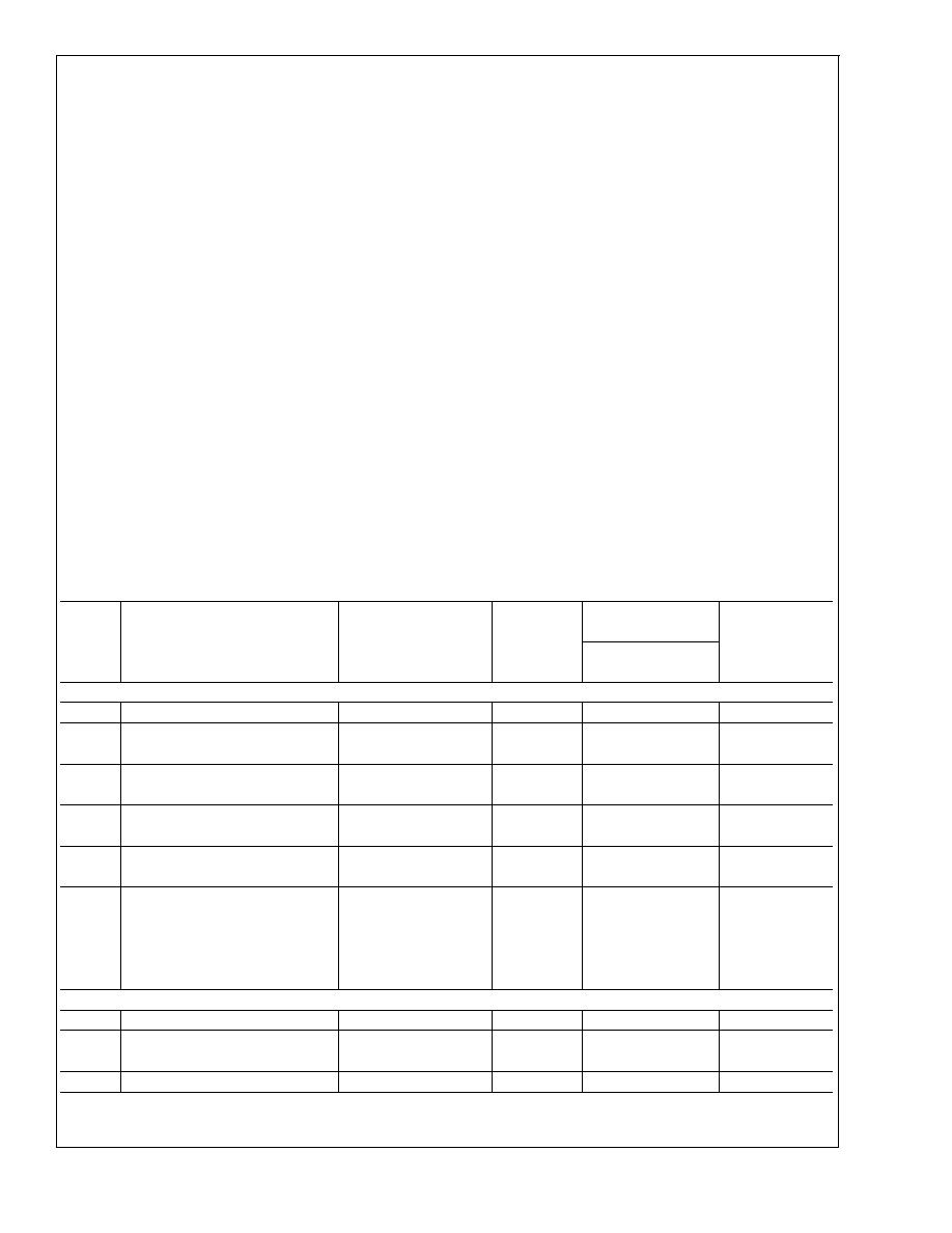
Absolute Maximum Ratings
(Notes 1, 3)
If Military/Aerospace specified devices are required,
please contact the National Semiconductor Sales Office/
Distributors for availability and specifications.
Positive Supply Voltage
(V
+
= AV
+
= DV
+
)
6.5V
Negative Supply Voltage (V
-
)
-6.5V
Total Supply Voltage (V
+
- V
-
)
13V
Total Reference Voltage
(V
REF
+
- V
REF
-
)
6.6V
Voltage at Inputs and
Outputs
V
-
- 0.3V to V
+
+ 0.3V
Input Current at Any Pin (Note 4)
±
5 mA
Package Input Current (Note 4)
±
20 mA
Package Dissipation at
T
A
= 25∞C (Note 5)
500 mW
ESD Susceptibility (Note 6)
2000V
Soldering Information
N Packages (10 Sec)
260∞C
J Packages (10 Sec)
300∞C
SO Package (Note 7):
Vapor Phase (60 Sec)
215∞C
Infrared (15 Sec)
220∞C
Storage Temperature
Ceramic DIP Packages
Plastic DIP and SO Packages
-65∞C to +150∞C
-40∞C to +150∞C
Operating Ratings
(Notes 2, 3)
Temperature Range
T
MIN
T
A
T
MAX
ADC10154CIWM,
ADC10158CIN,
ADC10158CIWM
-40∞C
T
A
+85∞C
Positive Supply
Voltage
(V
+
= AV
+
= DV
+
)
4.5 V
DC
to 5.5 V
DC
Unipolar Negative
Supply Voltage
(V
-
)
DGND
Bipolar Negative
Supply Voltage
(V
-
)
-4.5V to -5.5V
V
+
- V
-
11V
V
REF
+
AV
+
+ 0.05 V
DC
to V
-
- 0.05 V
DC
V
REF
-
AV
+
+ 0.05 V
DC
to V
-
- 0.05 V
DC
V
REF
(V
REF
+
- V
REF
-
)
0.5 V
DC
to V
+
Electrical Characteristics
The following specifications apply for V
+
= AV
+
= DV
+
= + 5.0 V
DC
, V
REF
+
= 5.000 V
DC
, V
REF
-
= GND, V
-
= GND for unipolar
operation or V
-
= -5.0 V
DC
for bipolar operation, and f
CLK
= 5.0 MHz unless otherwise specified. Boldface limits apply for T
A
= T
J
= T
MIN
to T
MAX
; all other limits T
A
= T
J
= 25∞C. (Notes 8, 9, 12)
Symbol
Parameter
Conditions
Typical
(Note 10)
CIN and CIWM
Units
(Limit)
Suffixes
Limits
(Note 11)
UNIPOLAR CONVERTER AND MULTIPLEXER STATIC CHARACTERISTICS
Resolution
10 + Sign
Bits
Unipolar Integral
V
REF
+
= 2.5V
±
0.5
LSB
Linearity Error
V
REF
+
= 5.0V
±
1
LSB (Max)
Unipolar Full-Scale Error
V
REF
+
= 2.5V
±
0.5
LSB
V
REF
+
= 5.0V
±
1.5
LSB (Max)
Unipolar Offset Error
V
REF
+
= 2.5V
±
1
LSB
V
REF
+
= 5.0V
±
2
LSB (Max)
Unipolar Total Unadjusted
V
REF
+
= 2.5V
±
1.5
LSB
Error (Note 13)
V
REF
+
= 5.0V
±
2.5
LSB (Max)
Unipolar Power Supply
V
+
= +5V
±
10%
Sensitivity
V
REF
+
= 4.5V
Offset Error
±
0.25
±
1
LSB (Max)
Full-Scale Error
±
0.25
±
1
LSB (Max)
Integral Linearity Error
±
0.25
LSB
BIPOLAR CONVERTER AND MULTIPLEXER STATIC CHARACTERISTICS
Resolution
10 + Sign
Bits
Bipolar Integral
V
REF
+
= 5.0V
±
1
LSB (Max)
Linearity Error
Bipolar Full-Scale Error
V
REF
+
= 5.0V
±
1.25
LSB (Max)
ADC10154/ADC10158
www.national.com
3

Electrical Characteristics
(Continued)
The following specifications apply for V
+
= AV
+
= DV
+
= + 5.0 V
DC
, V
REF
+
= 5.000 V
DC
, V
REF
-
= GND, V
-
= GND for unipolar
operation or V
-
= -5.0 V
DC
for bipolar operation, and f
CLK
= 5.0 MHz unless otherwise specified. Boldface limits apply for T
A
= T
J
= T
MIN
to T
MAX
; all other limits T
A
= T
J
= 25∞C. (Notes 8, 9, 12)
Symbol
Parameter
Conditions
Typical
(Note 10)
CIN and CIWM
Units
(Limit)
Suffixes
Limits
(Note 11)
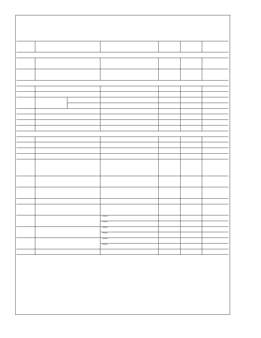
BIPOLAR CONVERTER AND MULTIPLEXER STATIC CHARACTERISTICS
Bipolar Negative Full-Scale
V
REF
+
= 5.0V
Error with Positive-Full
±
1.25
LSB (Max)
Scale Adjusted
Bipolar Offset Error
V
REF
+
= 5.0V
±
2.5
LSB (Max)
Bipolar Total Unadjusted
V
REF
+
= 5.0V
±
3
LSB (Max)
Error (Note 13)
Bipolar Power Supply
Sensitivity
Offset Error
V
+
= +5V
±
10%
±
0.5
±
2.5
LSB (Max)
Full-Scale Error
V
REF
+
= 4.5V
±
0.5
±
1.5
LSB (Max)
Integral Linearity Error
±
0.25
LSB
Offset Error
V
-
= -5V
±
10%
±
0.25
±
0.75
LSB (Max)
Full-Scale Error
V
REF
+
= 4.5V
±
0.25
±
0.75
LSB (Max)
Integral Linearity Error
±
0.25
LSB
UNIPOLAR AND BIPOLAR CONVERTER AND MULTIPLEXER STATIC CHARACTERISTICS
Missing Codes
0
DC Common Mode
V
IN
+
= V
IN
-
Error (Note 14)
= V
IN
where
Bipolar
+5.0V
V
IN
-5.0V
±
0.25
±
0.75
LSB (Max)
Unipolar
+5.0V
V
IN
0V
±
0.25
±
0.5
LSB (Max)
R
REF
Reference Input Resistance
7
4.5
k
(Max)
9.5
k
(Max)
C
REF
Reference Input Capacitance
70
pF
V
AI
Analog Input Voltage
(V
+
+0.05)
V (Max)
(V
-
-0.05)
V (Min)
C
AI
Analog Input Capacitance
30
pF
Off Channel Leakage
On Channel = 5V
-400
-1000
nA (Max)
Current
Off Channel = 0V
(Note 15)
On Channel = 0V
400
1000
nA (Max)
Off Channel = 5V
Electrical Characteristics
The following specifications apply for V
+
= AV
+
= DV
+
= + 5.0 V
DC
, V
REF
+
= 5.000 V
DC
, V
REF
-
= GND, V
-
= GND for unipolar
operation or V
-
= -5.0 V
DC
for bipolar operation, and f
CLK
= 5.0 MHz unless otherwise specified. Boldface limits apply for T
A
= T
J
= T
MIN
to T
MAX
; all other limits T
A
= T
J
= 25∞C. (Notes 8, 9, 12)
Symbol
Parameter
Conditions
Typical
Limits
(Note 11)
Units
(Limit)
(Note 10)
DYNAMIC CONVERTER AND MULTIPLEXER CHARACTERISTICS
S/(N+D)
Unipolar Signal-to-Noise+
f
IN
= 10 kHz, V
IN
= 4.85 V
p≠p
60
dB
Distortion Ratio
f
IN
= 150 kHz, V
IN
= 4.85 V
p-p
58
dB
S/(N+D)
Bipolar Signal-to-Noise+
f
IN
= 10 kHz, V
IN
=
±
4.85V
60
dB
Distortion Ratio
f
IN
= 150 kHz, V
IN
=
±
4.85V
58
dB
ADC10154/ADC10158
www.national.com
4
Electrical Characteristics
(Continued)
The following specifications apply for V
+
= AV
+
= DV
+
= + 5.0 V
DC
, V
REF
+
= 5.000 V
DC
, V
REF
-
= GND, V
-
= GND for unipolar
operation or V
-
= -5.0 V
DC
for bipolar operation, and f
CLK
= 5.0 MHz unless otherwise specified. Boldface limits apply for T
A
= T
J
= T
MIN
to T
MAX
; all other limits T
A
= T
J
= 25∞C. (Notes 8, 9, 12)
Symbol
Parameter
Conditions
Typical
Limits
(Note 11)
Units
(Limit)
(Note 10)
DYNAMIC CONVERTER AND MULTIPLEXER CHARACTERISTICS
-3 dB Unipolar Full
V
IN
= 4.85 V
p≠p
200
kHz
Power Bandwidth
-3 dB Bipolar Full
V
IN
=
±
4.85V
200
kHz
Power Bandwidth
REFERENCE CHARACTERISTICS (Unipolar Operation V
-
= GND Only)
VREFOut
Reference Output Voltage
2.5
±
1%
2.5
±
2%
V (Max)
V
REF
/
t
VREFOut Temperature Coefficient
40
ppm/∞C
V
REF
/
I
L
Load Regulation
Sourcing
0 mA
I
L
+4 mA
0.003
0.1
%/mA (Max)
Sinking
0 mA
I
L
-1 mA
0.2
0.6
%/mA (Max)
Line Regulation
4.5V
V
+
5.5V
0.5
6
mV (Max)
I
SC
Short Circuit Current
VREFOut = 0V
14
25
mA (Max)
V
REF
/
t
Long-Term Stability
200
ppm/1 kHr
t
SU
Start-Up Time
C
L
= 330 µF
20
ms
DIGITAL AND DC CHARACTERISTICS
V
IN(1)
Logical "1" Input Voltage
V
+
= 5.5V
2.0
V (Min)
V
IN(0)
Logical "0" Input Voltage
V
+
= 4.5V
0.8
V (Max)
I
IN(1)
Logical "1" Input Current
V
IN
= 5.0V
0.005
2.5
µA (Max)
I
IN(0)
Logical "0" Input Current
V
IN
= 0V
-0.005
-2.5
µA (Max)
V
OUT(1)
Logical "1" Output Voltage
V
+
= 4.5V:
I
OUT
= -360 µA
2.4
V (Min)
I
OUT
= -10 µA
4.25
V (Min)
V
OUT(0)
Logical "0" Output Voltage
V
+
= 4.5V
0.4
V (Max)
I
OUT
= 1.6 mA
I
OUT
TRI-STATE Output Current
V
OUT
= 0V
-0.01
-3
µA (Max)
V
OUT
= 5V
0.01
3
µA (Max)
+I
SC
Output Short Circuit Source Current
V
OUT
= 0V
-40
-10
mA (Min)
-I
SC
Output Short Circuit
V
OUT
= DV
+
30
10
mA (Min)
Sink Current
DI+
Digital Supply Current
CS = HIGH
0.75
2
mA (Max)
CS = HIGH, f
CLK
= 0 Hz
0.15
mA (Max)
AI
+
Analog Supply Current
CS = HIGH
3
4.5
mA (Max)
CS = HIGH, f
CLK
= 0 Hz
3
mA (Max)
I
-
Negative Supply Current
CS = HIGH
3.5
4.5
mA (Max)
CS = HIGH, f
CLK
= 0 Hz
3.5
mA (Max)
I
REF
Reference Input Current
V
REF
+
= 5V
0.7
1.1
mA (Max)
ADC10154/ADC10158
www.national.com
5