 | –≠–ª–µ–∫—Ç—Ä–æ–Ω–Ω—ã–π –∫–æ–º–ø–æ–Ω–µ–Ω—Ç: ADC1061 | –°–∫–∞—á–∞—Ç—å:  PDF PDF  ZIP ZIP |

ADC1061
10-Bit High-Speed µP-Compatible A/D Converter with
Track/Hold Function
General Description
Using a modified half-flash conversion technique, the 10-bit
ADC1061 CMOS analog-to-digital converter offers very fast
conversion times yet dissipates a maximum of only 235 mW.
The ADC1061 performs a 10-bit conversion in two
lower-resolution "flashes", thus yielding a fast A/D without
the cost, power dissipation, and other problems associated
with true flash approaches.
The analog input voltage to the ADC1061 is tracked and held
by an internal sampling circuit. Input signals at frequencies
from DC to greater than 160 kHz can therefore be digitized
accurately without the need for an external sample-and-hold
circuit.
For ease of interface to microprocessors, the ADC1061 has
been designed to appear as a memory location or I/O port
without the need for external interface logic.
Features
n
1.8 µs maximum conversion time to 10 bits
n
Low power dissipation: 235 mW (maximum)
n
Built-in track-and-hold
n
No external clock required
n
Single +5V supply
n
No missing codes over temperature
Applications
n
Waveform digitizers
n
Disk drives
n
Digital signal processor front ends
n
Mobile telecommunications
Simplified Block and Connection Diagrams
TRI-STATE
Æ
is a registered trademark of National Semiconductor Corporation.
DS010559-2
June 1999
ADC1061
10-Bit
High-Speed
µP-Compatible
A/D
Converter
with
T
rack/Hold
Function
© 1999 National Semiconductor Corporation
DS010559
www.national.com

Simplified Block and Connection Diagrams
(Continued)
Ordering Information
Industrial (-40∞C
T
A
85∞C)
Package
ADC1061CIN
N20A
ADC1061CIWM
M20B
Pin Descriptions
Symbol
Function
DV
CC
,
AV
CC
(1, 6)
These are the digital and analog positive supply voltage inputs. They should always be connected to the
same voltage source, but are brought out separately to allow for separate bypass capacitors. Each
supply pin should be bypassed with a 0.1 µF ceramic capacitor in parallel with a 10 µF tantalum
capacitor.
INT (2)
This is the active low interrupt output. INT goes low at the end of each conversion, and returns to a high
state following the rising edge of RD .
S /H (3)
This is the Sample/Hold control input. When this pin is forced low, it causes the analog input signal to be
sampled and initiates a new conversion.
RD (4)
This is the active low Read control input. When this pin is low, any data present in the ADC1061's output
registers will be placed on the data bus. In Mode 2, the Read signal must be low until INT goes low. Until
INT goes low, the data at the output pins will be incorrect.
CS (5)
This is the active low Chip Select control input. This pin enables the S /H and RD inputs.
V
REF-
,
V
REF+
(7, 9)
These are the reference voltage inputs. They may be placed at any voltage between GND - 50 mV and
V
CC
+ 50 mV, but V
REF+
must be greater than V
REF-
. An input voltage equal to V
REF-
produces an
output code of 0, and an input voltage equal to V
REF+
- 1LSB produces an output code of 1023.
V
IN
(8)
This is the analog input pin. The impedance of the source should be less than 500
for best accuracy
and conversion speed. To avoid damage to the ADC1061, V
IN
should not be allowed to extend beyond
the power supply voltages by more than 300 mV unless the drive current is limited. For accurate
conversions, V
IN
should not extend more than 50 mV beyond the supply voltages.
GND (10)
This is the power supply ground pin. The ground pin should be connected to a "clean" ground reference
point.
DB0≠DB9
(11-20)
These are the TRI-STATE output pins.
Dual-In-Line Package
DS010559-1
Top View
Order Number
ADC1061CIN or ADC1061CIWM
See NS Package J20A,
M20B or N20A
www.national.com
2

Absolute Maximum Ratings
(Notes 1, 2)
If Military/Aerospace specified devices are required,
please contact the National Semiconductor Sales Office/
Distributors for availability and specifications.
Supply Voltage (V
+
= AV
CC
= DV
CC
)
-0.3V to +6V
Voltage at any Input or Output
-0.3V to V
+
+0.3V
Input Current at Any Pin (Note 3)
5 mA
Package Input Current (Note 3)
20 mA
Power Dissipation (Note 4)
875 mW
ESD Susceptibility (Note 5)
1500V
Soldering Information (Note 6)
N Package (10 seconds)
260∞C
J Package (10 seconds)
300∞C
SO Package (Note 6)
Vapor Phase (60 seconds)
215∞C
Infrared (15 seconds)
220∞C
Junction Temperature, T
J
+150∞C
Storage Temperature Range
-65∞C to +150∞C
Operating Ratings
(Notes 1, 2)
Temperature Range
T
MIN
T
A
T
MAX
ADC1061CIN, ADC1061CIWM
-40∞C
T
A
+85∞C
Supply Voltage Range
4.5V to 5.5V
Converter Characteristics
The following specifications apply for V
+
= +5V, V
REF(+)
= 5V, and V
REF(-)
= GND unless otherwise specified. Boldface lim-
its apply for T
A
= T
J
= T
MIN
to T
MAX
; all other limits T
A
= T
J
= 25∞C.
Symbol
Parameter
Conditions
Typical
Limit
Units
(Note 7)
(Note 8)
(Limit)
Resolution
10
Bits
Total Unadjusted Error
±
1.0
±
2.0
LSB (Max)
Integral Linearity Error
±
0.3
±
1.5
LSB (Max)
Differential Linearity Error
±
1.0
LSB (Max)
Offset Error
±
0.1
±
1.0
LSB (Max)
Fullscale Error
±
0.5
±
1.0
LSB (Max)
R
REF
Reference Resistance
0.65
0.4
k
(Min)
R
REF
Reference Resistance
0.65
0.9
k
(Max)
V
REF(+)
V
REF(+)
Input Voltage
V
+
+ 0.05
V (Max)
V
REF(-)
V
REF(-)
Input Voltage
GND - 0.05
V (Min)
V
REF(+)
V
REF(+)
Input Voltage
V
REF(-)
V (Min)
V
REF(-)
V
REF(-)
Input Voltage
V
REF(-)
V (Max)
V
IN
Input Voltage
V
+
+ 0.05
V (Max)
V
IN
Input Voltage
GND - 0.05
V (Min)
Analog Input Leakage Current
CS = V
+
, V
IN
= V
+
0.01
3
µA (Max)
CS = V
+
, V
IN
= GND
0.01
-3
µA (Max)
Power Supply Sensitivity
V
+
= 5V
±
5%
±
0.125
±
0.5
LSB
V
REF
= 4.75V
DC Electrical Characteristics
The following specifications apply for V
+
= +5V, V
REF(+)
= 5V, and V
REF(-)
= GND unless otherwise specified. Boldface lim-
its apply for T
A
= T
J
= T
MIN
to T
MAX
; all other limits T
A
= T
J
= 25∞C.
Symbol
Parameter
Conditions
Typical
Limit
Units
(Note 7)
(Note 8)
(Limits)
V
IN(1)
Logical "1" Input Voltage
V
+
= 5.25V
2.0
V (Min)
V
IN(0)
Logical "0" Input Voltage
V
+
= 4.75V
0.8
V (Max)
I
IN(1)
Logical "1" Input Current
V
IN(1)
= 5V
0.005
1.0
µA (Max)
I
IN(0)
Logical "0" Input Current
V
IN(0)
= 0V
-0.005
-1.0
µA (Max)
V
OUT(1)
Logical "1" Output Voltage
V
+
= 4.75V I
OUT
= -360 µA
2.4
V (Min)
V
+
= 4.75V I
OUT
= -10 µA
4.5
V (Min)
V
OUT(0)
Logical "0" Output Voltage
V
+
= 4.75V I
OUT
= 1.6 mA
0.4
V (Max)
I
OUT
TRI-STATE
Æ
Output Current
V
OUT
= 5V
0.1
50
µA (Max)
V
OUT
= 0V
-0.1
-50
µA (Max)
DI
CC
DV
CC
Supply Current
CS = WR = RD = 0
0.1
2
mA (Max)
AI
CC
AV
CC
Supply Current
CS = WR = RD = 0
30
45
mA (Max)
www.national.com
3

AC Electrical Characteristics
The following specifications apply for V
+
= +5V, t
r
= t
f
= 20 ns, V
REF(+)
= 5V, and V
REF(-)
= GND unless otherwise specified.
Boldface limits apply for T
A
= T
J
= T
MIN
to T
MAX
; all other limits T
A
= T
J
= 25∞C.
Symbol
Parameter
Conditions
Typical
Limit
Units
(Note 7)
(Note 8)
(Limits)
t
CONV
Conversion Time from Rising Edge
Mode 1
1.2
1.8
µs (Max)
of S /H to Falling Edge of INT
t
CRD
Conversion Time for MODE 2
Mode 2
1.8
2.4
µs (Max)
(RD Mode)
t
ACC1
Access Time (Delay from Falling
Mode 1; C
L
= 100 pF
20
50
ns (Max)
Edge of RD to Output Valid)
t
ACC2
Access Time (Delay from Falling
Mode 2; C
L
= 100 pF
t
CRD
+ 50
ns (Max)
Edge of RD to Output Valid)
t
SH
Minimum Sample Time
(
Figure 1); (Note 9)
250
ns (Max)
t
1H
, t
0H
TRI-STATE Control (Delay from Rising
R
L
= 1k, C
L
= 10 pF
20
50
ns (Max)
Edge of RD to High-Z State)
t
INTH
Delay from Rising Edge of RD
10
50
ns (Max)
to Rising Edge of INT
t
ID
Delay from INT to Output Valid
C
L
= 100 pF
20
50
ns (Max)
t
P
Delay from End of Conversion
10
20
ns (Max)
to Next Conversion
SR
Slew Rate for Correct
2.5
V/µs
Track-and-Hold Operation
C
VIN
Analog Input Capacitance
35
pF
C
OUT
Logic Output Capacitance
5
pF
C
IN
Logic Input Capacitance
5
pF
Note 1: Absolute Maximum Ratings indicate limits beyond which damage to the device may occur. Operating Ratings indicate conditions for which the device is func-
tional, but do not guarantee specific performance limits. For guaranteed specifications and test conditions, see the Electrical Characteristics. The guaranteed speci-
fications apply only for the test conditions listed. Some performance characteristics may degrade when the device is not operated under the listed test conditions.
Note 2: All voltages are measured with respect to GND, unless otherwise specified.
Note 3: When the input voltage (V
IN
) at any pin exceeds the power supply rails (V
IN
<
V
-
or V
IN
>
V
+
) the absolute value of current at that pin should be limited
to 5 mA or less. The 20 mA package input current limits the number of pins that can safely exceed the power supplies with an input of 5 mA to four.
Note 4: The maximum power dissipation must be derated at elevated temperatures and is dictated by T
JMAX
,
JA
and the ambient temperature, T
A
. The maximum
allowable power dissipation at any temperature is P
D
= (T
JMAX
- T
A
)/
JA
or the number given in the Absolute Maximum Ratings, whichever is lower. For this device,
T
JMAX
= 150∞C, and the typical thermal resistance (
JA
) when board mounted is 47∞C/W for the plastic (N) package, 85∞C/W for the ceramic (J) package, and 65∞C/W
for the small outline (WM) package.
Note 5: Human body model, 100 pF discharged through a 1.5 k
resistor.
Note 6: See AN-450 "Surface Mounting Methods and Their Effect on Product Reliability" or the section titled "Surface Mount" found in a current National Semicon-
ductor Linear Data Book for other methods of soldering surface mount devices.
Note 7: Typicals are at 25∞C and represent most likely parametric norm.
Note 8: Limits are guaranteed to National's AOQL (Average Outgoing Quality Level).
Note 9: Accuracy may degrade if t
SH
is shorter than the value specified.
TRI-STATE Test Circuits and Waveforms
DS010559-3
DS010559-4
www.national.com
4
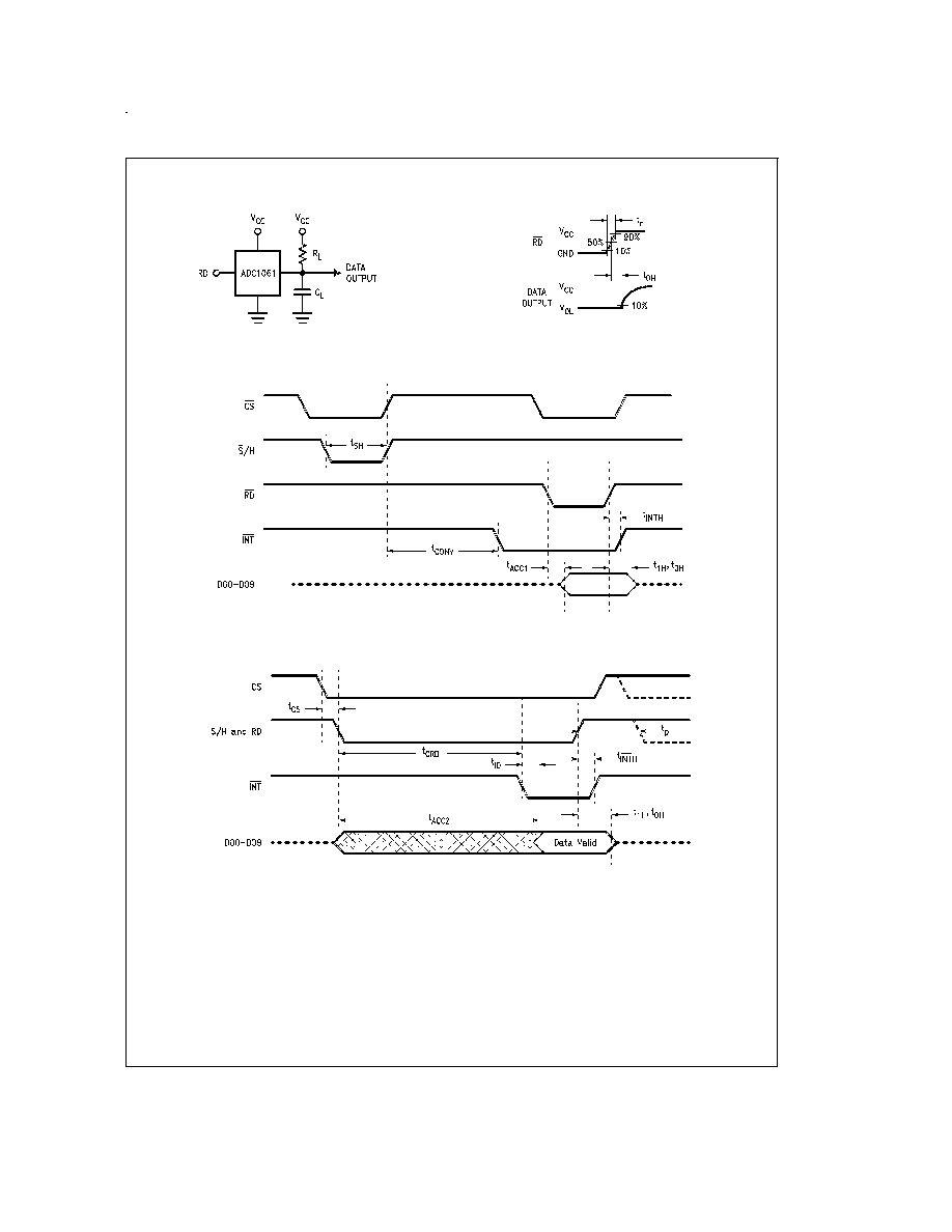
TRI-STATE Test Circuits and Waveforms
(Continued)
Timing Diagrams
DS010559-5
DS010559-6
DS010559-7
FIGURE 1. Mode 1. The conversion time (t
CONV
) is determined by the internal timer.
DS010559-8
FIGURE 2. Mode 2 (RD Mode). The conversion time (t
CRD
) includes
the sampling time, and is determined by the internal timer.
www.national.com
5