
ADC10731/ADC10732/ADC10734/ADC10738
10-Bit Plus Sign Serial I/O A/D Converters with Mux,
Sample/Hold and Reference
General Description
This series of CMOS 10-bit plus sign successive approxima-
tion A/D converters features versatile analog input multiplex-
ers, sample/hold and a 2.5V band-gap reference. The 1-, 2-,
4-, or 8-channel multiplexers can be software configured for
single-ended or differential mode of operation.
An input sample/hold is implemented by a capacitive refer-
ence ladder and sampled-data comparator. This allows the
analog input to vary during the A/D conversion cycle.
In the differential mode, valid outputs are obtained even
when the negative inputs are greater than the positive be-
cause of the 10-bit plus sign output data format.
The serial I/O is configured to comply with the NSC MI-
CROWIRE
TM
serial data exchange standard for easy inter-
face to the COPS
TM
and HPC
TM
families of controllers, and
can easily interface with standard shift registers and micro-
processors.
Features
n
0V to 5V analog input range with single 5V power
supply
n
Serial I/O (MICROWIRE compatible)
n
1-, 2-, 4-, or 8-channel differential or single-ended
multiplexer
n
Software or hardware power down
n
Analog input sample/hold function
n
Ratiometric or absolute voltage referencing
n
No zero or full scale adjustment required
n
No missing codes over temperature
n
TTL/CMOS input/output compatible
n
Standard DIP and SO packages
Key Specifications
n
Resolution
10 bits plus sign
n
Single supply
5V
n
Power dissipation
37 mW (Max)
n
In powerdown mode
18 �W
n
Conversion time
5�s (Max)
n
Sampling rate
74 kHz (Max)
n
Band-gap reference
2.5V
�
2% (Max)
Applications
n
Medical instruments
n
Portable and remote instrumentation
n
Test equipment
ADC10738 Simplified Block Diagram
COPS
TM
, HPC
TM
and MICROWIRE
TM
are trademarks of National Semiconductor Corporation.
DS011390-1
May 1999
ADC10731/ADC10732/ADC10734/ADC10738
10-Bit
Plus
Sign
Serial
I/O
A/D
Converters
with
Mux,
Sample/Hold
and
Reference
� 2001 National Semiconductor Corporation
DS011390
www.national.com

Connection Diagrams
DS011390-2
Top View
See NS Package Number M16B
DS011390-4
Top View
See NS Package Number M20B
DS011390-3
Top View
See NS Package Number M20B
DS011390-5
Top View
See NS Package Number M24B
SSOP Package
DS011390-34
See NS Package Number MSA20
ADC10731/ADC10732/ADC10734/ADC10738
www.national.com
2

Ordering Information
Industrial Temperature Range
Package
-40�C
T
A
+85�C
ADC10731CIWM
M16B
ADC10732CIWM
M20B
ADC10734CIMSA
MSA20
ADC10734CIWM
M20B
ADC10738CIWM
M24B
Pin Descriptions
CLK
The clock applied to this input controls the suc-
cessive approximation conversion time interval,
the acquisition time and the rate at which the
serial data exchange occurs. The rising edge
loads the information on the DI pin into the mul-
tiplexer address shift register. This address con-
trols which channel of the analog input multi-
plexer (MUX) is selected. The falling edge shifts
the data resulting from the A/D conversion out
on DO. CS enables or disables the above func-
tions. The clock frequency applied to this input
can be between 5 kHz and 3 MHz.
DI
This is the serial data input pin. The data applied
to this pln is shifted by CLK into the multiplexer
address register.
Tables 1, 2, 3 show the multi-
plexer address assignment.
DO
The data output pin. The A/D conversion result
(DB0-SIGN) are clocked out by the failing edge
of CLK on this pin.
CS
This is the chip select input pin. When a logic low
is applied to this pin, the rising edge of CLK
shifts the data on DI into the address register.
This low also brings DO out of TRI-STATE after
a conversion has been completed.
PD
This is the power down input pin. When a logic
high is applied to this pin the A/D is powered
down. When a low is applied the A/D is powered
up.
SARS
This is the successive approximation register
status output pin. When CS is high this pin is in
TRI-STATE. With CS low this pin is active high
when a conversion is in progress and active low
at all other times.
CH0�CH7 These are the analog inputs of the MUX. A chan-
nel input is selected by the address information
at the DI pin, which is loaded on the rising edge
of CLK into the address register (see
Tables 1, 2,
3).
The voltage applied to these inputs should not
exceed AV
+
or go below GND by more than
50 mV. Exceeding this range on an unselected
channel will corrupt the reading of a selected
channel.
COM
This pin is another analog input pln. It can be
used as a "pseudo ground" when the analog
multiplexer is single-ended.
V
REF
+
This is the positive analog voltage reference
input. In order to malntaln accuracy, the voltage
range V
REF
(V
REF
= V
REF
+�V
REF
-) is 0.5 V
DC
to
5.0 V
DC
and the voltage at V
REF
+ cannot exceed
AV
+
+50 mV.
V
REF
-
The negative voltage reference input. In order to
maintain accuracy, the voltage at this pin must
not go below GND - 50 mV or exceed AV
+
+ 50 mV.
AV
+
, DV
+
These are the analog and digital power supply
pins. These pins should be tied to the same
power supply and bypassed separately. The op-
erating voltage range of AV
+
and DV
+
is 4.5 V
DC
to 5.5 V
DC
.
DGND
This is the digital ground pin.
AGND
This is the analog ground pin.
ADC10731/ADC10732/ADC10734/ADC10738
www.national.com
3
Absolute Maximum Ratings
(Notes 1, 3)
If Military/Aerospace specified devices are required,
please contact the National Semiconductor Sales Office/
Distributors for availability and specifications.
Supply Voltage (V
+
= AV
+
= DV
+
)
6.5V
Total Reference Voltage
(V
REF
+�V
REF
-)
6.5V
Voltage at Inputs and Outputs
V
+
+ 0.3V to -0.3V
Input Current at Any Pin (Note 4)
30 mA
Package Input Current (Note 4)
120 mA
Package Dissipation at T
A
= 25�C
(Note 5)
500 mW
ESD Susceptability (Note 6)
Human Body Model
2500V
Machine Model
150V
Soldering Information
N packages (10 seconds)
260�C
SO Package (Note 7)
Vapor Phase (60 seconds)
215�C
Infrared (15 seconds)
220�C
Storage Temperature
-40�C to +150�C
Operating Ratings
(Notes 2, 3)
Operating Temperature Range
T
MIN
T
A
T
MAX
ADC10731CIWM,
ADC10732CIWM,
ADC10734CIWM,
ADC10734CIMSA,
ADC10738CIWM
-40�C
T
A
+85�C
Supply Voltage
(V
+
= AV
+
= DV
+
)
+4.5V to +5.5V
V
REF
+
AV
+
+50 mV to -50 mV
V
REF
-
AV
+
+50 mV to -50 mV
V
REF
(V
REF
+�V
REF
-)
+0.5V to V
+
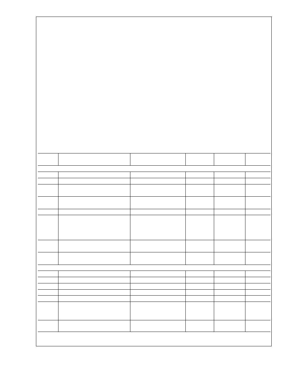
Electrical Characteristics
The following specifications apply for V
+
= AV
+
= DV
+
= +5.0 V
DC
, V
REF
+ = 2.5 V
DC
, V
REF
- = GND, V
IN
- = 2.5V for Signed
Characteristics, V
IN
- = GND for Unsigned Characteristics and f
CLK
= 2.5 MHz unless otherwise specified. Boldface limits ap-
ply for T
A
= T
J
= T
MIN
to T
MAX
; all other limits T
A
= T
J
= +25�C. (Notes 8, 9, 10)
Symbol
Parameter
Conditions
Typical
Limits
Units
(Note 11)
(Note 12)
(Limits)
SIGNED STATIC CONVERTER CHARACTERISTICS
Resolution with No Missing Codes
10 + Sign
Bits
TUE
Total Unadjusted Error (Note 13)
�
2.0
LSB(max)
INL
Positive and Negative Integral
�
1.25
LSB(max)
Linearity Error
Positive and Negative
�
1.5
LSB(max)
Full-Scale Error
Offset Error
�
1.5
LSB(max)
Power Supply Sensitivity
Offset Error
V
+
= +5.0V
�
10%
�
0.2
�
1.0
LSB(max)
+ Full-Scale Error
�
0.2
�
1.0
LSB(max)
- Full-Scale Error
�
0.1
�
0.75
LSB(max)
DC Common Mode Error (Note 14)
V
IN
+ = V
IN
- = V
IN
where
�
0.1
�
0.33
LSB(max)
5.0V
V
IN
0V
Multiplexer Channel to
�
0.1
LSB
Channel Matching
UNSIGNED STATIC CONVERTER CHARACTERISTICS
Resolution with No Missing Codes
10
Bits
TUE
Total Unadjusted Error (Note 13)
V
REF
+ = 4.096V
�
0.75
LSB
INL
Integral Linearity Error
V
REF
+ = 4.096V
�
0.50
LSB
Full-Scale Error
V
REF
+ = 4.096V
�
1.25
LSB(max)
Offset Error
V
REF
+ = 4.096V
�
1.25
LSB(max)
Power Supply Sensitivity
Offset Error
V
+
= +5.0V
�
10%
�
0.1
LSB
Full-Scale Error
V
REF
+ = 4.096V
�
0.1
LSB
DC Common Mode Error (Note 14)
V
IN
+ = V
IN
- = V
IN
where
+5.0V
V
IN
0V
�
0.1
LSB
ADC10731/ADC10732/ADC10734/ADC10738
www.national.com
4

Electrical Characteristics
(Continued)
The following specifications apply for V
+
= AV
+
= DV
+
= +5.0 V
DC
, V
REF
+ = 2.5 V
DC
, V
REF
- = GND, V
IN
- = 2.5V for Signed
Characteristics, V
IN
- = GND for Unsigned Characteristics and f
CLK
= 2.5 MHz unless otherwise specified. Boldface limits ap-
ply for T
A
= T
J
= T
MIN
to T
MAX
; all other limits T
A
= T
J
= +25�C. (Notes 8, 9, 10)
Symbol
Parameter
Conditions
Typical
Limits
Units
(Note 11)
(Note 12)
(Limits)
UNSIGNED STATIC CONVERTER CHARACTERISTICS
Multiplexer Channel to Channel
Matching
V
REF
+ = 4.096V
�
0.1
LSB
DYNAMIC SIGNED CONVERTER CHARACTERISTICS
S/(N+D)
Signal-to-Noise Plus Distortion Ratio
V
IN
= 4.85 V
PP
,
67
dB
and f
IN
= 1 kHz to 15 kHz
ENOB
Effective Number of Bits
V
IN
= 4.85 V
PP
,
10.8
Bits
and f
IN
= 1 kHz to 15 kHz
THD
Total Harmonic Distortion
V
IN
= 4.85 V
PP
,
-78
dB
and f
IN
= 1 kHz to 15 kHz
IMD
Intermodulation Distortion
V
IN
= 4.85 V
PP
,
-85
dB
and f
IN
= 1 kHz to 15 kHz
Full-Power Bandwidth
V
IN
= 4.85 V
PP
, where
380
kHz
S/(N + D) Decreases
3 dB
Multiplexer Channel to Channel
Crosstalk
f
IN
= 15 kHz
-80
dB
DYNAMIC UNSIGNED CONVERTER CHARACTERISTIC
S/(N+D)
Signal-to-Noise Plus Distortion Ratio
V
REF
+ = 4.096V,
V
IN
= 4.0 V
PP
, and
60
dB
f
IN
=1 kHz to 15 kHz
Effective Bits
V
REF
+ = 4.096V,
V
IN
= 4.0 V
PP
, and
9.8
Bits
f
IN
= 1 kHz to 15 kHz
THD
Total Harmonic Distortion
V
REF
+ = 4.096V,
V
IN
= 4.0 V
PP
, and
-70
dB
f
IN
= 1 kHz to 15 kHz
IMD
Intermodulation Distortion
V
REF
+ = 4.096V,
V
IN
= 4.0 V
PP
, and
-73
dB
f
IN
= 1 kHz to 15 kHz
Full-Power Bandwidth
V
IN
= 4.0 V
PP
,
V
REF
+ = 4.096V,
380
kHz
where S/(N+D) decreases
3 dB
Multiplexer Channel to Channel
f
IN
= 15 kHz,
-80
dB
Crosstalk
V
REF
+ = 4.096V
REFERENCE INPUT AND MULTIPLEXER CHARACTERISTICS
Reference Input Resistance
7
k
5.0
k
(min)
9.5
k
(max)
C
REF
Reference Input Capacitance
70
pF
MUX Input Voltage
-50
mV(min)
AV
+
+50 mV
(max)
C
IM
MUX Input Capacitance
47
pF
ADC10731/ADC10732/ADC10734/ADC10738
www.national.com
5