TL H 5676
ADC1205ADC1225
12-Bit
Plus
Sign
m
P
Compatible
AD
Converters
June 1994
ADC1205 ADC1225 12-Bit Plus Sign
mP Compatible A D Converters
General Description
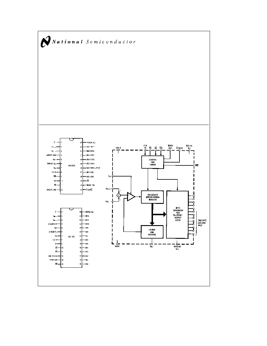
The ADC1205 and ADC1225 are CMOS 12-bit plus sign
successive approximation A D converters
The 24-pin
ADC1205 outputs the 13-bit data result in two 8-bit bytes
formatted high-byte first with sign extended The 28-pin
ADC1225 outputs a 13-bit word in parallel for direct inter-
face to a 16-bit data bus
Negative numbers are represented in 2's complement data
format All digital signals are fully TTL and MOS compatible
A unipolar input (0V to 5V) can be accommodated with a
single 5V supply while a bipolar input (
b
5V to
a
5V) re-
quires the addition of a 5V negative supply
The ADC1205C and ADC1225C have a maximum non-lin-
earity of 0 0224% of Full Scale
Key Specifications
Y
Resolution
12 bits plus sign
Y
Linearity Error
g
1 LSB
Y
Conversion Time
100 ms
Features
Y
Compatible with all mPs
Y
True differential analog voltage inputs
Y
0V to 5V analog voltage range with single 5V supply
Y
TTL MOS input output compatible
Y
Low power
25 mW max
Y
Standard 24-pin or 28-pin DIP
Connection and Functional Diagrams
Dual-In-Line Package
TL H 5676 ≠ 1
Top View
Dual-In-Line Package
TL H 5676 ≠ 2
Top View
TL H 5676 ≠ 3
See Ordering Information
TRI-STATE
is a registered trademark of National Semiconductor Corporation
C1995 National Semiconductor Corporation
RRD-B30M115 Printed in U S A
Absolute Maximum Ratings
(Notes 1
2)
If Military Aerospace specified devices are required
please contact the National Semiconductor Sales
Office Distributors for availability and specifications
Supply Voltage (DV
CC
and AV
CC
)
6 5V
Negative Supply Voltage (V
b
)
b
15V to GND
Logic Control Inputs
b
0 3V to
a
15V
Voltage at Analog Inputs
V
IN(a)
V
IN(b)
(V
b
)
b
0 3V to V
CC
a
0 3V
Voltage at All Outputs V
REF
V
OS
b
0 3V to (V
CC
a
0 3)V
Input Current per Pin
g
5mA
Input Current per Package
g
20mA
Storage Temperature Range
b
65 C to
a
150 C
Package Dissipation at T
A
e
25 C
875 mW
Lead Temp (Soldering 10 seconds)
300 C
ESD Susceptibility (Note 12)
800V
Operating Conditions
(Notes 1
2)
Temperature Range
T
MIN
s
T
A
s
T
MAX
ADC1205CCJ ADC1225CCD
b
40 C
s
T
A
s
a
85 C
ADC1205CCJ-1 ADC1225CCD-1
0 C
s
T
A
s
70 C
Supply Voltage (DV
CC
and AV
CC
)
4 5 V
DC
to 6 0 V
DC
Negative Supply Voltage (V
b
)
b
15V to GND
Electrical Characteristics
The following specifications apply for DV
CC
e
AV
CC
e
5V V
REF
e
5V f
CLK
e
1 0 MHz V
b
e b
5V for bipolar input range or
V
b
e
GND for unipolar input range unless otherwise specified Bipolar input range is defined as
b
5 05V
s
V
IN(a)
s
5 05V
b
5 05V
s
V
IN(b)
s
5 05V and
l
V
IN(a)
b
V
IN(b)
l
s
5 05V Unipolar input range is defined as
b
0 05V
s
V
IN(a)
s
5 05V
b
0 05V
s
V
IN(b)
s
5 05V and
l
V
IN(a)
b
V
IN(b)
l
s
5 05V Boldface limits apply from T
MIN
to T
MAX
all other limits T
A
e
T
J
e
25 C (Notes 3 4 5 6 7)
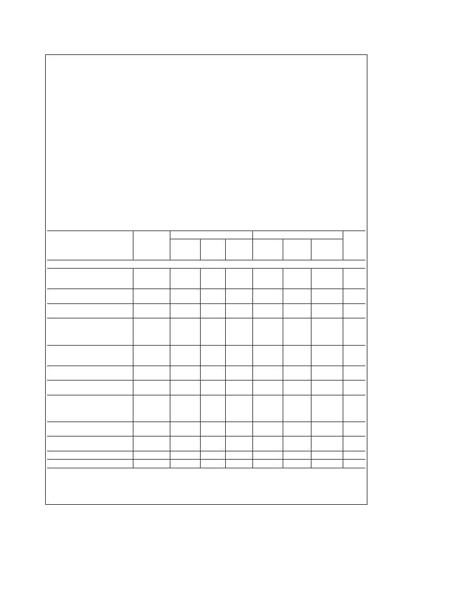
Parameter
Conditions
ADC1205CCJ ADC1225CCD
ADC1205CCJ-1 ADC1225CCD-1
Units
Limit
Typ
Tested
Design
Typ
Tested
Design
(Note 8)
Limit
Limit
(Note 8)
Limit
Limit
(Note 9) (Note 10)
(Note 9)
(Note 10)
CONVERTER CHARACTERISTICS
Linearity Error
Unipolar Input
ADC1205CCJ ADC1225CCD
Range
g
1
LSB
ADC1205CCJ-1 ADC1225CCD-1 (Note 11)
g
1
g
1
LSB
Unadjusted Zero Error
Unipolar Input
g
2
g
2
g
2
LSB
Range
Unadjusted Positive and Negative
Unipolar Input
g
30
g
30
g
30
LSB
Full-Scale Error
Range
Negative Full-Scale Error
Unipolar Input
g
g
LSB
Range Full
Scale Adj to
Zero
Linearity Error
Bipolar Input
ADC1205CCJ ADC1225CCD
Range
g
2
LSB
ADC1205CCJ-1 ADC1225CCD-1 (Note 11)
g
2
g
2
LSB
Unadjusted Zero Error
Bipolar Input
g
2
g
2
g
2
LSB
Range
Unadjusted Positive and Negative
Bipolar Input
g
30
g
30
g
30
LSB
Full-Scale Error
Range
Negative Full-Scale Error
Bipolar Input
g
2
g
2
g
2
LSB
Range Full
Scale Adj to
Zero
Maximum Gain Temperature
6
15
6
15
ppm C
Coefficient
Maximum Offset Temperature
0 5
1 5
0 5
1 5
ppm C
Coefficient
Minimum V
REF
Input Resistance
4 0
2
4 0
2
2
kX
Maximum V
REF
Input Resistance
4 0
8
4 0
8
8
kX
2
Electrical Characteristics
(Continued)
The following specifications apply for DV
CC
e
AV
CC
e
5V V
REF
e
5V f
CLK
e
1 0 MHz V
b
e b
5V for bipolar input range or
V
b
e
GND for unipolar input range unless otherwise specified Bipolar input range is defined as
b
5 05V
s
V
IN(a)
s
5 05V
b
5 05V
s
V
IN(b)
s
5 05V and
l
V
IN(a)
b
V
IN(b)
l
s
5 05V Unipolar input range is defined as
b
0 05V
s
V
IN(a)
s
5 05V
b
0 05V
s
V
IN(b)
s
5 05V and
l
V
IN(a)
b
V
IN(b)
l
s
5 05V Boldface limits apply from T
MIN
to T
MAX
all other limits T
A
e
T
J
e
25 C (Notes 3 4 5 6 7)
Parameter
Conditions
ADC1205CCJ ADC1225CCD
ADC1205CCJ-1 ADC1225CCD-1
Units
Limit
Typ
Tested
Design
Typ
Tested
Design
(Note 8)
Limit
Limit
(Note 8)
Limit
Limit
(Note 9)
(Note 10)
(Note 9)
(Note 10)
CONVERTER CHARACTERISTICS
(Continued)
Minimum Analog Input
Unipolar Input
GND-0 05
GND-0 05
GND-0 05
V
Voltage
Range
Bipolar Input
b
V
CC
b
0 05
b
V
C
b
0 05
b
V
CC
b
0 05
V
Range
Maximum Analog Input
Unipolar Input
V
CC
a
0 05
V
CC
a
0 05
V
CC
a
0 05
V
Voltage
Range
Bipolar Input
V
CC
a
0 05
V
CC
a
0 05
V
CC
a
0 05
V
Range
DC Common-Mode Error
g
g
g
g
g
LSB
Power Supply Sensitivity
AV
CC
e
DV
CC
e
5V
g
5%
V
b
e b
5V
g
5%
Zero Error
g
g
g
LSB
Positive and Negative
g
g
g
LSB
Full-Scale Error
Linearity Error
g
g
g
LSB
DIGITAL AND DC CHARACTERISTICS
V
IN(1)
Logical ``1'' Input
V
CC
e
5 25V
2 0
2 0
2 0
V
Voltage (Min)
All Inputs except
CLK IN
V
IN(0)
Logical ``0'' Input
V
CC
e
4 75V
0 8
0 8
0 8
V
Voltage (Max)
All Inputs except
CLK IN
I
IN(1)
Logical ``1'' Input
V
IN
e
5V
0 005
1
0 005
1
mA
Current (Max)
I
IN(0)
Logical ``0'' Input
V
IN
e
0V
b
0 005
b
1
b
0 005
b
1
mA
Current (Max)
V
T
a
(Min) Minimum Positive-
CLK IN
3 1
2 7
3 1
2 7
2 7
V
Going Threshold Voltage
V
T
a
(Max) Maximum Positive- CLK IN
3 1
3 5
3 1
3 5
3 5
V
Going Threshold Voltage
V
T
b
(Min) Minimum Negative-
CLK IN
1 8
1 4
1 8
1 4
1 4
V
Going Threshold Voltage
V
T
b
(Max) Maximum Negative- CLK IN
1 8
2 1
1 8
2 1
2 1
V
Going Threshold Voltage
V
H
(Min) Minimum Hysteresis
CLK IN
1 3
0 6
1 3
0 6
0 6
V
V
T
a
(Min)
b
V
T
b
(Max)
V
H
(Max) Maximum Hysteresis
CLK IN
1 3
2 1
1 3
2 1
2 1
V
V
T
a
(Max)
b
V
T
b
(Min)
3
Electrical Characteristics
(Continued)
The following specifications apply for DV
CC
e
AV
CC
e
5V V
REF
e
5V f
CLK
e
1 0 MHz V
b
e b
5V for bipolar input range or
V
b
e
GND for unipolar input range unless otherwise specified Bipolar input range is defined as
b
5 05V
s
V
IN(a)
s
5 05V
b
5 05V
s
V
IN(b)
s
5 05V and
l
V
IN(a)
b
V
IN(b)
l
s
5 05V Unipolar input range is defined as
b
0 05V
s
V
IN(a)
s
5 05V
b
0 05V
s
V
IN(b)
s
5 05V and
l
V
IN(a)
b
V
IN(b)
l
s
5 05V Boldface limits apply from T
MIN
to T
MAX
all other limits T
A
e
T
J
e
25 C (Notes 3 4 5 6 7)
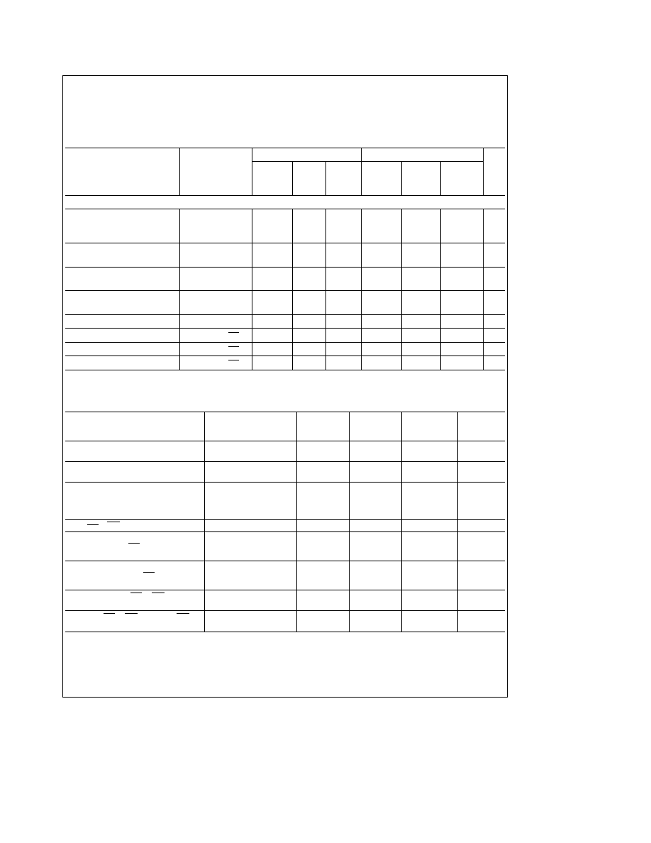
Parameter
Conditions
ADC1205CCJ ADC1225CCD
ADC1205CCJ-1 ADC1225CCD-1
Units
Limit
Typ
Tested
Design
Typ
Tested
Design
(Note 8)
Limit
Limit
(Note 8)
Limit
Limit
(Note 9) (Note 10)
(Note 9)
(Note 10)
DIGITAL AND DC CHARACTERISTICS
(Continued)
V
OUT(1)
Logical ``1'' Output
V
CC
e
4 75V
Voltage (Min)
I
OUT
e b
360 mA
2 4
2 4
2 4
V
I
OUT
e b
10 mA
4 5
4 5
4 5
V
V
OUT(0)
Logical ``0'' Output
V
CC
e
4 75V
0 4
0 4
0 4
V
Voltage (Max)
I
OUT
e
1 6 mA
I
OUT
TRI-STATE Output Leakage V
OUT
e
0V
b
0 01
b
3
b
0 01
b
0 3
b
3
m
A
Current (Max)
V
OUT
e
5V
0 01
3
0 01
0 3
3
m
A
I
SOURCE
Output Source Current
V
OUT
e
0V
b
12
b
6 0
b
12
b
7 0
b
6 0
mA
(Min)
I
SINK
Output Sink Current (Min)
V
OUT
e
5V
16
8 0
16
9 0
8 0
mA
DI
CC
DV
CC
Supply Current (Max) f
CLK
e
1 MHz CS
e
1
1
3
1
2 5
3
mA
AI
CC
AV
CC
Supply Current (Max) f
CLK
e
1 MHz CS
e
1
1
3
1
2 5
3
mA
I
b
V
b
Supply Current (Max)
f
CLK
e
1 MHz CS
e
1
10
100
10
100
100
m
A
AC Electrical Characteristics
The following specifications apply for DV
CC
e
AV
CC
e
5 0V t
r
e
t
f
e
20 ns and T
A
e
25 C unless otherwise specified
Typ
Tested
Design
Limit
Parameter
Conditions
(Note 8)
Limit
Limit
Units
(Note 9)
(Note 10)
f
CLK
Clock Frequency
MIN
1 0
0 3
MHz
MAX
1 0
1 5
MHz
Clock Duty Cycle
MIN
40
%
MAX
60
%
T
C
Conversion Time
MIN
108
1 f
CLK
MAX
109
1 f
CLK
MIN
f
CLK
e
1 0 MHz
108
m
s
MAX
f
CLK
e
1 0 MHz
109
m
s
t
W(WR)L
WR Pulse Width
MAX
220
350
ns
t
ACC
Access Time (Delay from
C
L
e
100 pF
210
340
ns
Falling Edge of RD to
Output Data Valid) (Max)
t
1H
t
0H
TRI-STATE Control (Delay
R
L
e
2k C
L
e
100 pF
170
290
ns
from Rising Edge of RD to
Hi-Z State) (Max)
t
PD(READYOUT)
RD or WR to
250
400
ns
READYOUT Delay (Max)
t
PD(INT)
RD or WR to Reset of INT
250
400
ns
(Max)
Note 1
Absolute Maximum Ratings indicate limits beyond which damage to the device may occur DC and AC electrical specifications do not apply when operating
the device beyond its specified operating ratings
Note 2
All voltages are measured with respect to ground unless otherwise specified
Note 3
A parasitic zener diode exists internally from AV
CC
and DV
CC
to ground This parasitic zener has a typical breakdown voltage of 7 V
DC
4
AC Electrical Characteristics
(Continued)
Note 4
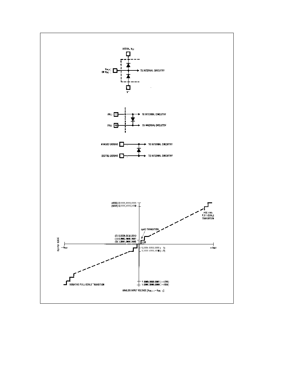
Two on-chip diodes are tied to each analog input as shown below
TL H 5676 ≠ 4
Errors in the A D conversion can occur if these diodes are forward biased more than 50 mV This means that if AV
CC
and DV
CC
are minimum (4 75 V
DC
) and V
b
is
minimum (
b
4 75V
DC
) full-scale must be
s
4 8V
DC
Note 5
A diode exists between analog V
CC
and digital V
C
TL H 5676 ≠ 20
To guarantee accuracy it is required that the AV
CC
and DV
CC
be connected together to a power supply with separate bypass filters at each V
CC
pin
Note 6
A diode exists between analog ground and digital ground
TL H 5676 ≠ 21
To guarantee accuracy it is required that the analog ground and digital ground be connected together externally
Note 7
Accuracy is guaranteed at f
CLK
e
1 0 MHz At higher clock frequencies accuracy may degrade
Note 8
Typicals are at 25 C and represent most likely parametric norm
Note 9
Tested and guaranteed to National's AOQL (Average Outgoing Quality Level)
Note 10
Guaranteed but not 100% production tested These limits are not used to calculate outgoing quality levels
Note 11
Linearity error is defined as the deviation of the analog value expressed in LSBs from the straight line which passes through positive full scale and zero
after adjusting zero error (See
Figures 1b and 1c )
Note 12
Human body model 100 pF discharged through a 1 5 kX resistor
TL H 5676 ≠ 8
FIGURE 1a Transfer Characteristic
5