TL H 11017
ADC12441
Dynamically-Tested
Self-Calibrating
12-Bit
Plus
Sign
AD
Converter
with
Sample-and-Hold
November 1994
ADC12441 Dynamically-Tested Self-Calibrating 12-Bit
Plus Sign A D Converter with Sample-and-Hold
General Description
The ADC12441 is a CMOS 12-bit plus sign successive ap-
proximation analog-to-digital converter whose dynamic
specifications (S N THD etc ) are tested and guaranteed
On request the ADC12441 goes through a self-calibration
cycle that adjusts positive linearity and full-scale errors to
less than
g
LSB each and zero error to less than
g
1 LSB The ADC12441 also has the ability to go through
an Auto-Zero cycle that corrects the zero error during every
conversion
The analog input to the ADC12441 is tracked and held by
the internal circuitry and therefore does not require an ex-
ternal sample-and-hold A unipolar analog input voltage
range (0V to
a
5V) or a bipolar range (
b
5V to
a
5V) can be
accommodated with
g
5V supplies
The 13-bit word on the outputs of the ADC12441 gives a 2's
complement representation of negative numbers The digi-
tal inputs and outputs are compatible with TTL or CMOS
logic levels
Features
Y
Self-calibration provides excellent temperature stability
Y
Internal sample-and-hold
Y
Bipolar input range with single
a
5V reference
Applications
Y
Digital signal processing
Y
Telecommunications
Y
Audio
Y
High resolution process control
Y
Instrumentation
Key Specifications
Y
Resolution
12 bits plus sign
Y
Conversion Time
13 8 ms (max)
Y
Bipolar Signal Noise
76 5 dB (min)
Y
Total Harmonic Distortion
b
75 dB (max)
Y
Aperture Time
100 ns
Y
Aperture Jitter
100 ps
rms
Y
Zero Error
g
1 LSB (max)
Y
Positive Full Scale Error
g
1 LSB (max)
Y
Power Consumption
g
5V
70 mW (max)
Y
Sampling rate
55 kHz (max)
TRI-STATE
is a registered trademark of National Semiconductor Corporation
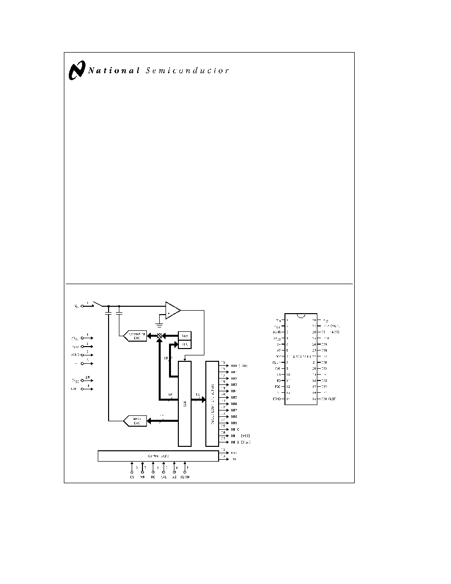
Simplified Block Diagram
TL H 11017 ≠ 1
Connection Diagram
Dual-In-Line Package
TL H 11017 ≠ 2
Top View
Order Number
ADC12441CMJ ADC12441CMJ 883
or ADC12441CIJ
See NS Package Number J28A
C1995 National Semiconductor Corporation
RRD-B30M115 Printed in U S A
Absolute Maximum Ratings
(Notes 1
2)
If Military Aerospace specified devices are required
please contact the National Semiconductor Sales
Office Distributors for availability and specifications
Supply Voltage (V
CC
e
DV
CC
e
AV
CC
)
6 5V
Negative Supply Voltage (V
b
)
b
6 5V
Voltage at Logic Control Inputs
b
0 3V to (V
CC
a
0 3V)
Voltage at Analog Inputs
(V
IN
and V
REF
)
(V
b
b
0 3V) to (V
CC
a
0 3V)
AV
CC
≠ DV
CC
(Note 7)
0 3V
Input Current at Any Pin (Note 3)
g
5 mA
Package Input Current (Note 3)
g
20 mA
Power Dissipation at 25 C (Note 4)
875 mW
Storage Temperature Range
b
65 C to
a
150 C
ESD Susceptability (Note 5)
2000V
Soldering Information
J Package (10 sec )
300 C
Operating Ratings
(Notes 1
2)
Temperature Range
T
MIN
s
T
A
s
T
MAX
ADC12441CIJ
b
40 C
s
T
A
s
a
85 C
ADC12441CMJ
ADC12441CMJ 883
b
55 C
s
T
A
s
a
125 C
DV
CC
and AV
CC
Voltage
(Notes 6
7)
4 5V to 5 5V
Negative Supply Voltage (V
b
)
b
4 5V to
b
5 5V
Reference Voltage
(V
REF
Notes 6
7)
3 5V to AV
CC
a
50 mV
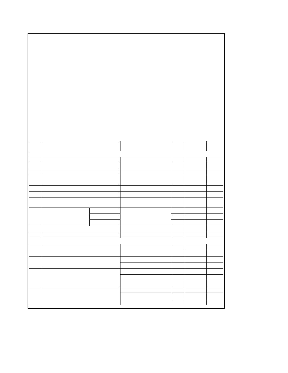
Converter Electrical Characteristics
The following specifications apply for V
CC
e
DV
CC
e
AV
CC
e a
5 0V V
b
e b
5 0V V
REF
e a
5 0V Analog Input Source
Impedance
e
600X and f
CLK
e
2 0 MHz unless otherwise specified Boldface limits apply for T
A
e
T
J
e
T
MIN
to T
MAX
all other limits T
A
e
T
J
e
25 C (Notes 6 7 and 8)
Symbol
Parameter
Conditions
Typical
Limit
Units
(Note 9)
(Note 10)
(Limit)
STATIC CHARACTERISTICS
Positive Integral Linearity Error
After Auto-Cal (Notes 11
12)
g
LSB
Negative Integral Linearity Error
After Auto-Cal (Notes 11
12)
g
LSB
Positive or Negative Differential Linearity
After Auto-Cal (Notes 11
12)
12
Bits
Zero Error
After Auto-Zero or Auto-Cal
g
1
LSB (max)
(Notes 12
13)
Positive Full-Scale Error
After Auto-Cal (Note 12)
g
g
1
LSB (max)
Negative Full-Scale Error
After Auto-Cal (Note 12)
g
1
g
2
LSB (max)
V
IN
Analog Input Voltage
V
b
b
0 05
V(min)
V
CC
a
0 05
V(max)
Power Supply
Zero Error (Note 14) AV
CC
e
DV
CC
e
5V
g
5%
g
LSB
Sensitivity
Full-Scale Error
V
REF
e
4 75V V
b
e b
5V
g
5%
g
LSB
Linearity Error
g
LSB
C
REF
V
REF
Input Capacitance (Note 18)
80
pF
C
IN
Analog Input Capacitance
65
pF
DYNAMIC CHARACTERISTICS
Bipolar Effective Bits
f
IN
e
1 kHz V
IN
e
g
4 85V
12 6
Bits
(Note 17)
f
IN
e
20 kHz V
IN
e
g
4 85V
12 6
12 4
Bits (min)
Unipolar Effective Bits
f
IN
e
1 kHz V
IN
e
4 85 V
p-p
11 8
Bits
(Note 17)
f
IN
e
20 kHz V
IN
e
4 85 V
p-p
11 8
11 6
Bits (min)
S N
Bipolar Signal-to-Noise Ratio
f
IN
e
1 kHz V
IN
e
g
4 85V
78
dB
(Note 17)
f
IN
e
10 kHz V
IN
e
g
4 85V
78
dB
f
IN
e
20 kHz V
IN
e
g
4 85V
78
76 5
dB (min)
S N
Unipolar Signal-to-Noise Ratio
f
IN
e
1 kHz V
IN
e
4 85 V
p-p
73
dB
(Note 17)
f
IN
e
10 kHz V
IN
e
4 85 V
p-p
73
dB
f
IN
e
20 kHz V
IN
e
4 85 V
p-p
73
71 5
dB (min)
2
Converter Electrical Characteristics
The following specifications apply for V
CC
e
DV
CC
e
AV
CC
e a
5 0V V
b
e b
5 0V V
REF
e a
5 0V Analog Input Source
Impedance
e
600X and f
CLK
e
2 0 MHz unless otherwise specified Boldface limits apply for T
A
e
T
J
e
T
MIN
to T
MAX
all other limits T
A
e
T
J
e
25 C (Notes 6 7 and 8) (Continued)
Symbol
Parameter
Conditions
Typical
Limit
Units
(Note 9) (Notes 10 19)
(Limit)
DYNAMIC CHARACTERISTICS
(Continued)
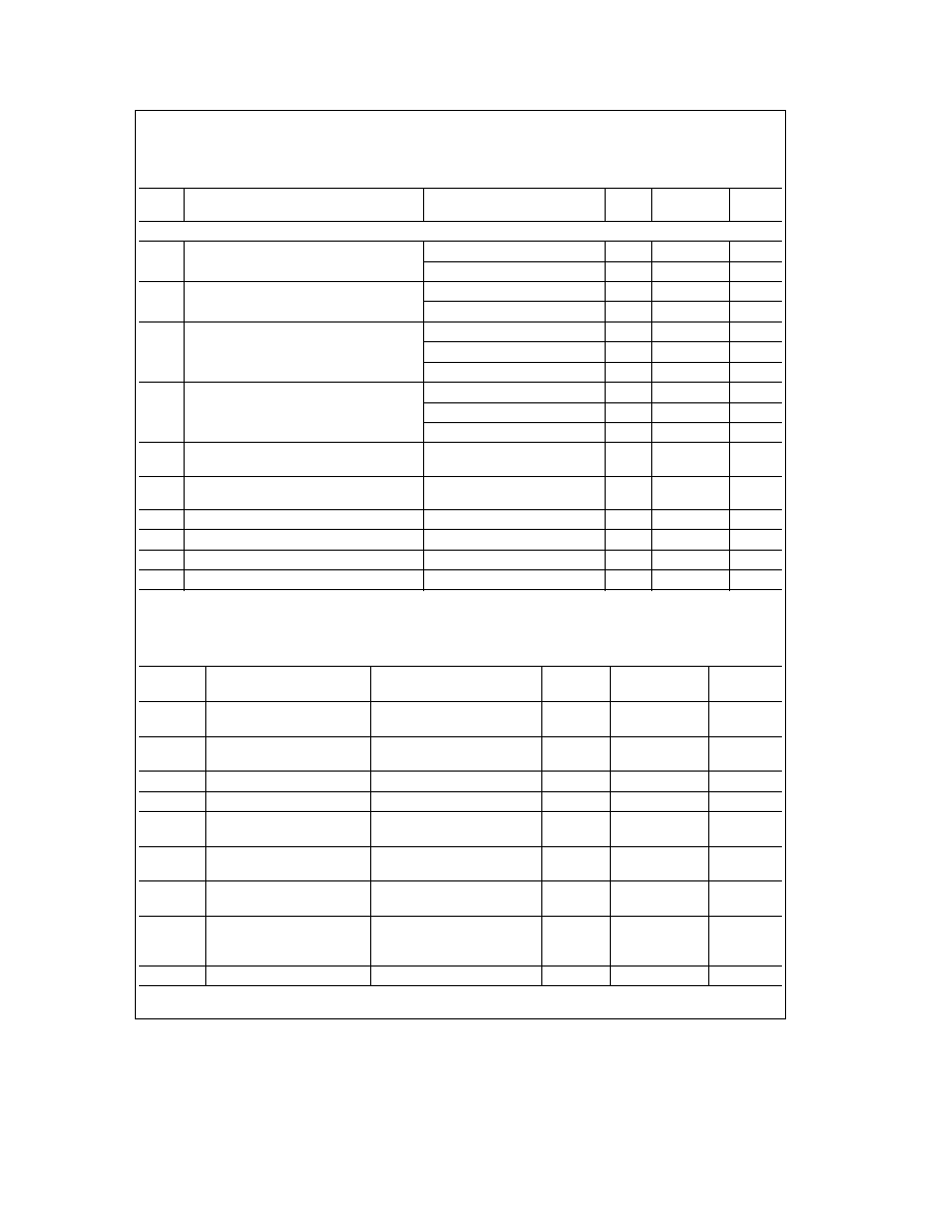
THD
Bipolar Total Harmonic Distortion
f
IN
e
1 kHz V
IN
e
g
4 85V
b
82
dB
(Note 17)
f
IN
e
19 688 kHz V
IN
e
g
4 85V
b
80
b
75
dB (max)
THD
Unipolar Total Harmonic Distortion
f
IN
e
1 kHz V
IN
e
4 85 V
p-p
b
82
dB
(Note 17)
f
IN
e
19 688 kHz V
IN
e
4 85 V
p-p
b
80
b
75
dB (max)
Bipolar Peak Harmonic or
f
IN
e
1 kHz V
IN
e
g
4 85V
b
88
dB
Spurious Noise (Note 17)
f
IN
e
10 kHz V
IN
e
g
4 85V
b
84
dB
f
IN
e
20 kHz V
IN
e
g
4 85V
b
80
dB
Unipolar Peak Harmonic or
f
IN
e
1 kHz V
IN
e
4 85 V
p-p
b
90
dB
Spurious Noise (Note 17)
f
IN
e
10 kHz V
IN
e
4 85 V
p-p
b
86
dB
f
IN
e
20 kHz V
IN
e
4 85 V
p-p
b
82
dB
Bipolar Two Tone Intermodulation
V
IN
e
g
4 85V f
IN1
e
19 375 kHz
b
78
b
74
dB (max)
Distortion (Note 17)
f
IN2
e
20 625 kHz
Unipolar Two Tone Intermodulation
V
IN
e
4 85 V
p-p
f
IN1
e
19 375 kHz
b
78
b
73
dB (max)
Distortion (Note 17)
f
IN2
e
20 625 kHz
b
3 dB Bipolar Full Power Bandwidth
V
IN
e
g
4 85V (Note 17)
25
20
kHz (Min)
b
3 dB Unipolar Full Power Bandwidth
V
IN
e
4 85 V
p-p
(Note 17)
30
20
kHz (Min)
Aperture Time
100
ns
Aperture Jitter
100
ps
rms
Digital and DC Electrical Characteristics
The following specifications apply for DV
CC
e
AV
CC
e a
5 0V V
b
e b
5 0V V
REF
e a
5 0V and f
CLK
e
2 0 MHz unless
otherwise specified Boldface limits apply for T
A
e
T
J
e
T
MIN
to T
MAX
all other limits T
A
e
T
J
e
25 C
(Notes 6 and 7)
Symbol
Parameter
Conditions
Typical
Limit
Units
(Note 9)
(Notes 10 19)
(Limits)
V
IN(1)
Logical ``1'' Input Voltage for
V
CC
e
5 25V
2 0
V (min)
All Inputs except CLK IN
V
IN(0)
Logical ``0'' Input Voltage for
V
CC
e
4 75V
0 8
V (max)
All Inputs except CLK IN
I
IN(1)
Logical ``1'' Input Current
V
IN
e
5V
0 005
1
m
A (max)
I
IN(0)
Logical ``0'' Input Current
V
IN
e
0V
b
0 005
b
1
m
A (max)
V
T
a
CLK IN Positive-Going
2 8
2 7
V (min)
Threshold Voltage
V
T
b
CLK IN Negative-Going
2 1
2 3
V (max)
Threshold Voltage
V
H
CLK IN Hysteresis
0 7
0 4
V (min)
V
T
a
(min)
b
V
T
b
(max)
V
OUT(1)
Logical ``1'' Output Voltage
V
CC
e
4 75V
I
OUT
e b
360 mA
2 4
V (min)
I
OUT
e b
10 mA
4 5
V (min)
V
OUT(0)
Logical ``0'' Output Voltage
V
CC
e
4 75V I
OUT
e
1 6 mA
0 4
V (max)
3
Digital and DC Electrical Characteristics
The following specifications apply for DV
CC
e
AV
CC
e a
5 0V V
b
e b
5 0V V
REF
e a
5 0V and f
CLK
e
2 0 MHz unless
otherwise specified Boldface limits apply for T
A
e
T
J
e
T
MIN
to T
MAX
all other limits T
A
e
T
J
e
25 C
(Notes 6 and 7) (Continued)
Symbol
Parameter
Conditions
Typical
Limit
Units
(Note 9)
(Notes 10 19)
(Limits)
I
OUT
TRI-STATE Output Leakage
V
OUT
e
0V
b
0 01
b
3
m
A (max)
Current
V
OUT
e
5V
0 01
3
m
A (max)
I
SOURCE
Output Source Current
V
OUT
e
0V
b
20
b
6 0
mA (min)
I
SINK
Output Sink Current
V
OUT
e
5V
20
8 0
mA (min)
DI
CC
DV
CC
Supply Current
f
CLK
e
2 MHz CS
e
``1''
1
2
mA (max)
AI
CC
AV
CC
Supply Current
f
CLK
e
2 MHz CS
e
``1''
2 8
6
mA (max)
I
b
V
b
Supply Current
f
CLK
e
2 MHz CS
e
``1''
2 8
6
mA (max)
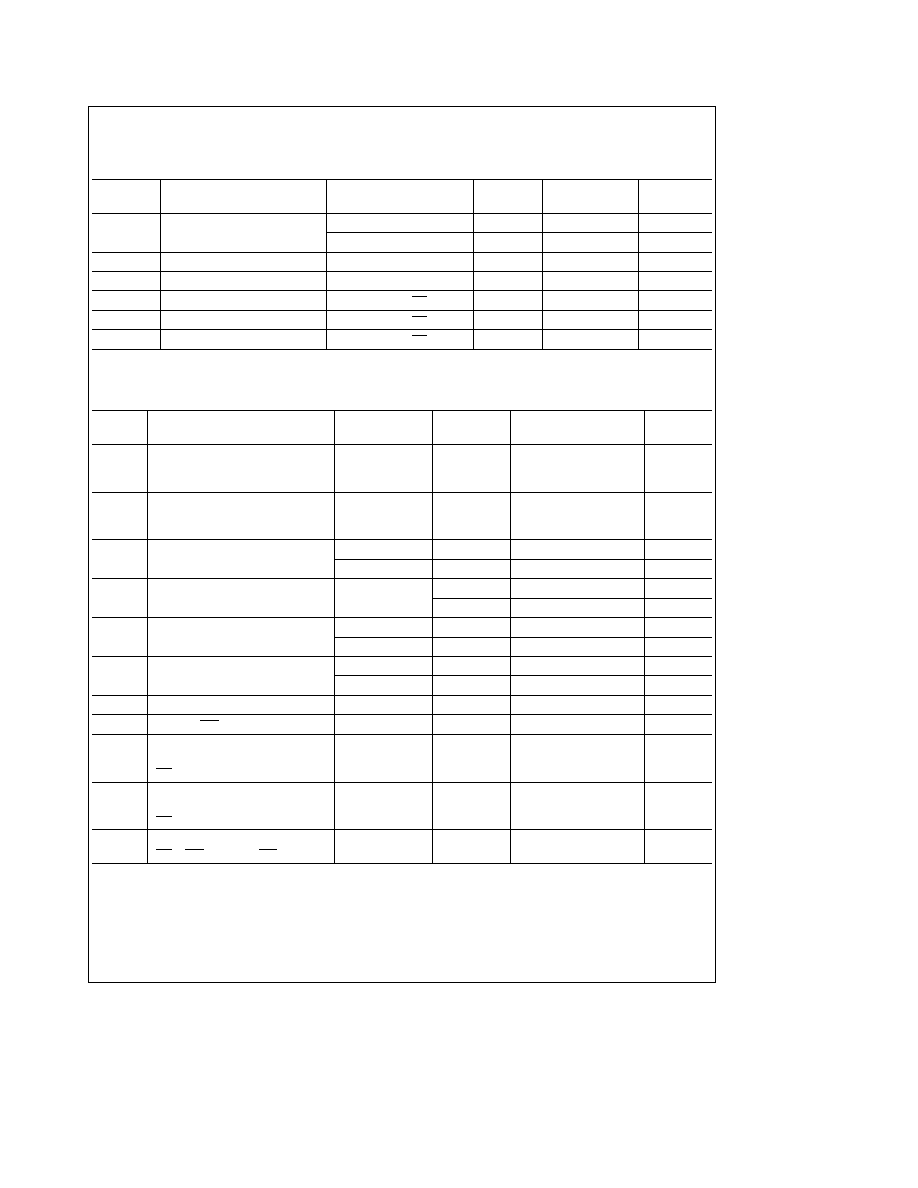
AC Electrical Characteristics
The following specifications apply for DV
CC
e
AV
CC
e
a
5 0V V
b
e
b
5 0V t
r
e
t
f
e
20 ns unless otherwise specified
Boldface limits apply for T
A
e
T
J
e
T
MIN
to T
MAX
all other limits T
A
e
T
J
e
25 C (Notes 6 and 7)
Symbol
Parameter
Conditions
Typical
Limit
Units
(Note 9)
(Notes 10 19)
(Limits)
f
CLK
Clock Frequency
0 5
MHz (min)
4 0
2 0
MHz (max)
Clock Duty Cycle
50
%
40
% (min)
60
% (max)
t
C
Conversion Time
27(1 f
CLK
)
27(1 f
CLK
)
a
300 ns
(max)
f
CLK
e
2 0 MHz
13 5
m
s
t
A
Acquisition Time
R
SOURCE
e
50X
7(1 f
CLK
)
7(1 f
CLK
)
a
300 ns
(max)
(Note 15)
f
CLK
e
2 0 MHz
3 5
m
s
t
Z
Auto Zero Time
26(1 f
CLK
)
26(1 f
CLK
)
(max)
f
CLK
e
2 0 MHz
13
m
s
t
CAL
Calibration Time
1396(1 f
CLK
)
max
f
CLK
e
2 0 MHz
698
706
m
s (max)
t
W(CAL)L
Calibration Pulse Width
(Note 16)
60
200
ns (min)
t
W(WR)L
Minimum WR Pulse Width
60
200
ns (min)
t
ACC
Maximum Access Time
C
L
e
100 pF
(Delay from Falling Edge of
50
85
ns (max)
RD to Output Data Valid)
t
0H
t
1H
TRI-STATE Control
R
L
e
1 kX
(Delay from Rising Edge of
C
L
e
100 pF
30
90
ns (max)
RD to Hi-Z State)
t
PD(INT)
Maximum Delay from Falling Edge of
100
175
ns (max)
RD or WR to Reset of INT
Note 1
Absolute Maximum Ratings indicate limits beyond which damage to the device may occur Operating Ratings indicate conditions for which the device is
functional but do not guarantee specific performance limits For guaranteed specifications and test conditions see the Electrical Characteristics The guaranteed
specifications apply only for the test conditions listed Some performance characteristics may degrade when the device is not operated under the listed test
conditions
Note 2
All voltages are measured with respect to AGND and DGND unless otherwise specified
Note 3
When the input voltage (V
IN
) at any pin exceeds the power supply rails (V
IN
k
V
b
or V
IN
l
(AV
CC
or DV
CC
) the current at that pin should be limited to
5 mA The 20 mA maximum package input current rating allows the voltage at any four pins with an input current limit of 5 mA to simultaneously exceed the power
supply voltages
4
AC Electrical Characteristics
(Continued)
Note 4
The power dissipation of this device under normal operation should never exceed 169 mW (Quiescent Power Dissipation
a
TTL Loads on the digital
outputs) Caution should be taken not to exceed absolute maximum power rating when the device is operating in a severe fault condition (ex when any inputs or
outputs exceed the power supply) The maximum power dissipation must be derated at elevated temperatures and is dictated by T
Jmax
(maximum junction
temperature) i
JA
(package junction to ambient thermal resistance) and T
A
(ambient temperature) The maximum allowable power dissipation at any temperature
is P
Dmax
e
(T
Jmax
b
T
A
) i
JA
or the number given in the Absolute Maximum Ratings whichever is lower For this device T
Jmax
e
125 C and the typical thermal
resistance (i
JA
) of the ADC12441 with CMJ and CIJ suffixes when board mounted is 47 C W
Note 5
Human body model 100 pF discharged through a 1 5 kX resistor
Note 6
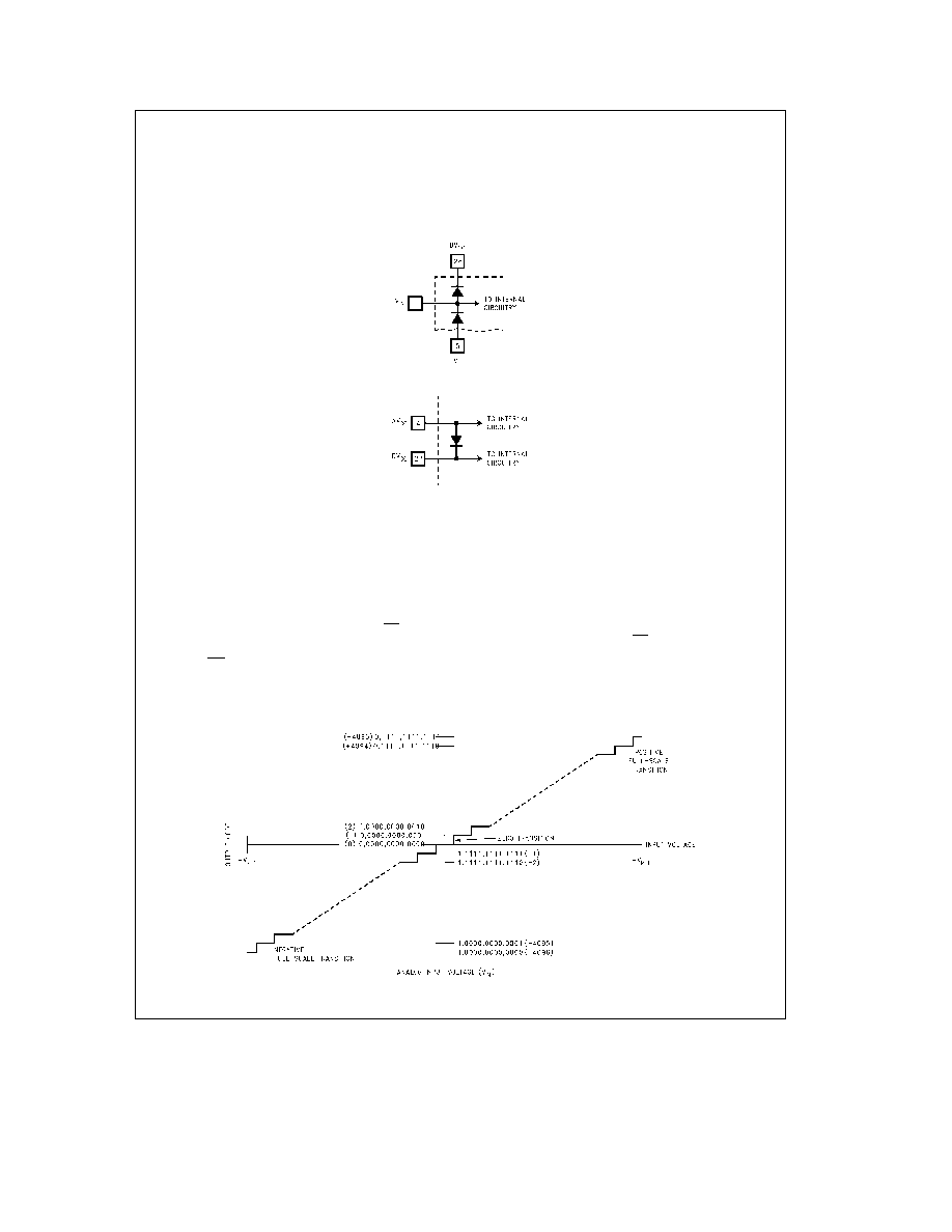
Two on-chip diodes are tied to the analog input as shown below Errors in the A D conversion can occur if these diodes are forward biased more than
50 mV
TL H 11017 ≠ 3
This means that if AV
CC
and DV
CC
are minimum (4 75 V
DC
) and V
b
is maximum (
b
4 75 V
DC
) full-scale must be
s
4 8 V
DC
Note 7
A diode exists between AV
CC
and DV
CC
as shown below
TL H 11017 ≠ 4
To guarantee accuracy it is required that the AV
CC
and DV
CC
be connected together to a power supply with separate bypass filters at each V
CC
pin
Note 8
Accuracy is guaranteed at f
CLK
e
2 0 MHz At higher and lower clock frequencies accuracy may degrade See curves in the Typical Performance
Characteristics section
Note 9
Typicals are at T
J
e
25 C and represent most likely parametric norm
Note 10
Limits are guaranteed to National's AOQL (Average Outgoing Quality Level)
Note 11
Positive linearity error is defined as the deviation of the analog value expressed in LSBs from the straight line that passes through positive full scale and
zero For negative linearity error the straight line passes through negative full scale and zero (See
Figures 1b and 1c )
Note 12
The ADC12441's self-calibration technique ensures linearity full scale and offset errors as specified but noise inherent in the self-calibration process will
result in a repeatability uncertainty of
g
0 20 LSB
Note 13
If T
A
changes then an Auto-Zero or Auto-Cal cycle will have to be re-started (see the Typical Performance Characteristic curves)
Note 14
After an Auto-Zero or Auto-Cal cycle at the specified power supply extremes
Note 15
If the clock is asynchronous to the falling edge of WR an uncertainty of one clock period will exist in the interval of t
A
therefore making the minimum
t
A
e
6 clock periods and the maximum t
A
e
7 clock periods If the falling edge of the clock is synchronous to the rising edge of WR then t
A
will be exactly 6 5 clock
periods
Note 16
The CAL line must be high before a conversion is started
Note 17
The specifications for these parameters are valid after an Auto-Cal cycle has been completed
Note 18
The ADC12441 reference ladder is composed solely of capacitors
Note 19
A Military RETS Electrical Test Specification is available on request At time of printing the ADC12441CMJ 883 RETS complies fully with the boldface
limits in this column
TL H 11017 ≠ 5
FIGURE 1a Transfer Characteristic
5