ADC12L030/ADC12L032/ADC12L034/ADC12L038
3.3V Self-Calibrating 12-Bit Plus Sign Serial I/O A/D
Converters with MUX and Sample/Hold
General Description
The ADC12L030 family is 12-bit plus sign successive ap-
proximation A/D converters with serial I/O and configurable
input multiplexers. These devices are fully tested with a
single 3.3V power supply. The ADC12L032, ADC12L034 and
ADC12L038 have 2, 4 and 8 channel multiplexers, respec-
tively. Differential multiplexer outputs and A/D inputs are
available on the MUXOUT1, MUXOUT2, A/DIN1 and A/DIN2
pins. The ADC12L030 has a two channel multiplexer with the
multiplexer outputs and A/D inputs internally connected. On
request, these A/Ds go through a self calibration process
that adjusts linearity, zero and full-scale errors to less than
±
1
/
2
LSB each.
The analog inputs can be configured to operate in various
combinations
of
single-ended,
differential,
or
pseudo-differential modes. A fully differential unipolar analog
input range (0V to +3.3V) can be accommodated with a
single +3.3V supply. In the differential modes, valid outputs
are obtained even when the negative inputs are greater than
the positive because of the 12-bit plus sign two's compliment
output data format.
The serial I/O is configured to comply with NSC's
MICROWIRE
TM
and Motorola's SPI standards. For voltage
references, see the LM4040 or LM4041 data sheets.
Features
n
0V to 3.3V analog input range with single 3.3V power
supply
n
Serial I/O ( MICROWIRE and SPI Compatible)
n
2, 4, or 8 channel differential or single-ended multiplexer
n
Analog input sample/hold function
n
Power down mode
n
Variable resolution and conversion rate
n
Programmable acquisition time
n
Variable digital output word length and format
n
No zero or full scale adjustment required
n
Fully tested and guaranteed with a 2.5V reference
n
No Missing Codes over temperature
Key Specifications
n
Resolution
12-bit plus sign
n
12-bit plus sign conversion time
8.8 µs (min)
n
12-bit plus sign sampling rate
73 kHz (max)
n
Integral linearity error
±
1 LSB (max)
n
Single supply
3.3V
±
10%
n
Power dissipation
15 mW (max)
n
Power down
40 µW (typ)
Applications
n
Portable Medical instruments
n
Portable computing
n
Portable Test equipment
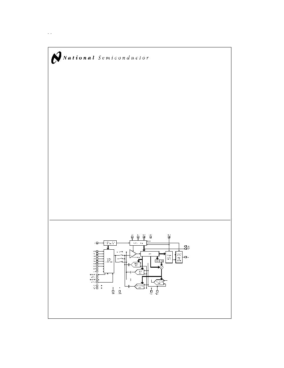
ADC12L038 Simplified Block Diagram
TRI-STATE
Æ
is a registered trademark of National Semiconductor Corporation.
COPS
TM
microcontrollers, HPC
TM
and MICROWIRE
TM
are trademarks of National Semiconductor Corporation.
Microsoft
TM
is a trademark of Microsoft Corporation.
DS011830-1
June 1999
ADC12L030/ADC12L032/ADC12L034/ADC12L038
3.3V
Self-Calibrating
12-Bit
Plus
Sign
Serial
I/O
A/D
Converters
with
MUX
and
Sample/Hold
© 1999 National Semiconductor Corporation
DS011830
www.national.com
Ordering Information
Industrial Temperature Range
NS Package
-40∞C
T
A
+85∞C
Number
ADC12L030CIWM
M16B
ADC12L032CIWM
M20B
ADC12L034CIWM
M24B
ADC12L038CIWM
M28B
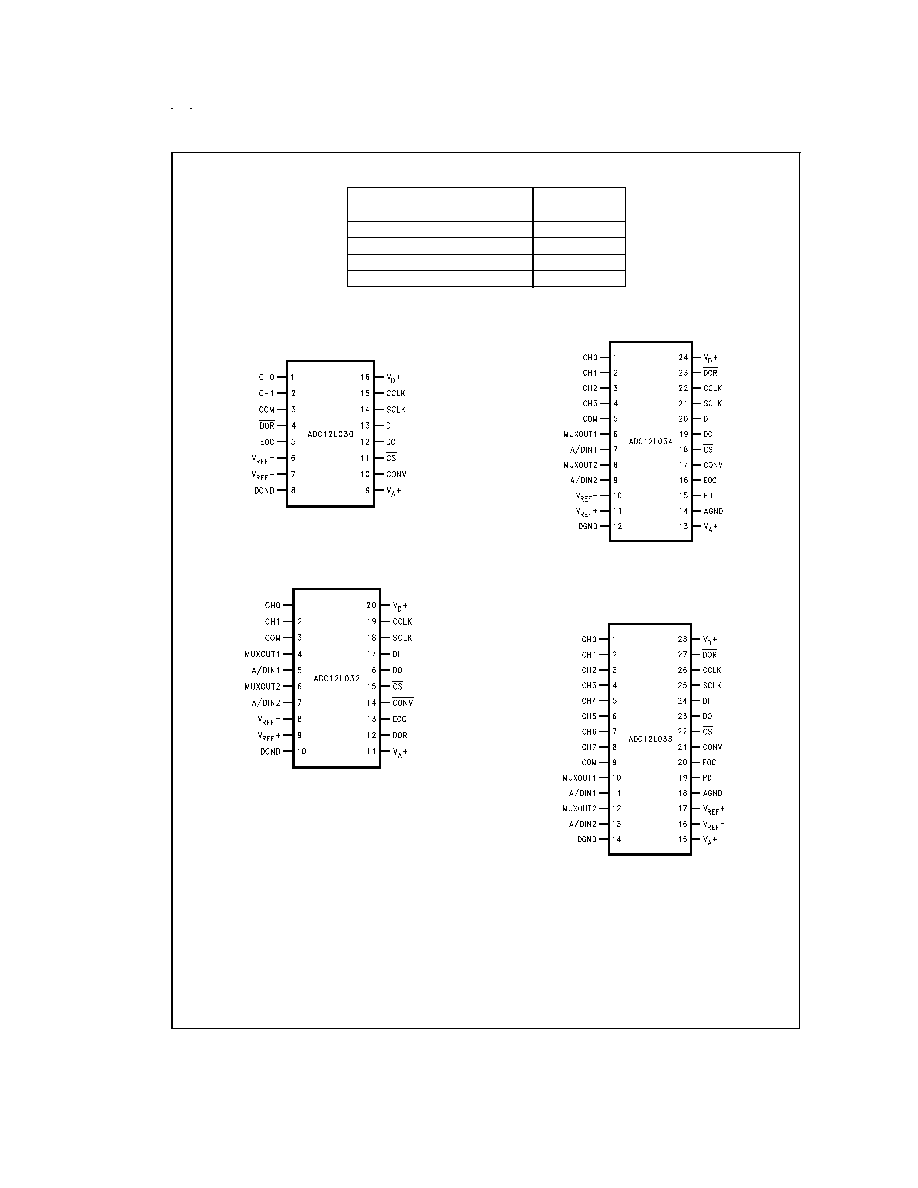
Connection Diagrams
16-Pin Wide Body
SO Packages
DS011830-2
Top View
20-Pin Wide Body
SO Packages
DS011830-3
Top View
24-Pin Wide Body
SO Packages
DS011830-4
Top View
248-Pin Wide Body
SO Packages
DS011830-5
Top View
www.national.com
2
Pin Descriptions
CCLK
The clock applied to this input controls the su-
cessive approximation conversion time interval
and the acquisition time. The rise and fall times
of the clock edges should not exceed 1 µs.
SCLK
This is the serial data clock input. The clock
applied to this input controls the rate at which
the serial data exchange occurs. The rising
edge loads the information on the DI pin into
the multiplexer address and mode select shift
register. This address controls which channel
of the analog input multiplexer (MUX) is se-
lected and the mode of operation for the A/D.
With CS low the falling edge of SCLK shifts the
data resulting from the previous ADC conver-
sion out on DO, with the exception of the first
bit of data. When CS is low continuously, the
first bit of the data is clocked out on the rising
edge of EOC (end of conversion). When CS is
toggled the falling edge of CS always clocks
out the first bit of data. CS should be brought
low when SCLK is low. The rise and fall times
of the clock edges should not exceed 1 µs.
DI
This is the serial data input pin. The data ap-
plied to this pin is shifted by the rising edge of
SCLK into the multiplexer address and mode
select register.
Tables 2, 3, 4, 5 show the as-
signment of the multiplexer address and the
mode select data.
DO
The data output pin. This pin is an active push/
pull output when CS is Low. When CS is High
this output is in TRI-STATE. The A/D conver-
sion result (D0≠D12) and converter status data
are clocked out by the falling edge of SCLK on
this pin. The word length and format of this re-
sult can vary (see
Table 1). The word length
and format are controlled by the data shifted
into the multiplexer address and mode select
register (see
Table 5).
EOC
This pin is an active push/pull output and indi-
cates the status of the ADC12L030/2/4/8.
When low, it signals that the A/D is busy with a
conversion,
auto-calibration,
auto-zero
or
power down cycle. The rising edge of EOC sig-
nals the end of one of these cycles.
CS
This is the chip select pin. When a logic low is
applied to this pin, the rising edge of SCLK
shifts the data on DI into the address register.
This low also brings DO out of TRI-STATE.
With CS low the falling edge of SCLK shifts the
data resulting from the previous ADC conver-
sion out on DO, with the exception of the first
bit of data. When CS is low continuously, the
first bit of the data is clocked out on the rising
edge of EOC (end of conversion). When CS is
toggled the falling edge of CS always clocks
out the first bit of data. CS should be brought
low when SCLK is low. The falling edge of CS
resets a conversion in progress and starts the
sequence for a new conversion. When CS is
brought back low during a conversion, that
conversion is prematurely ended. The data in
the output latches may be corrupted. There-
fore, when CS is brought back low during a
conversion in progress the data output at that
time should be ignored. CS may also be left
continuously low. In this case it is imperative
that the correct number of SCLK pulses be ap-
plied to the ADC in order to remain synchro-
nous. After the ADC supply power is applied, it
expects to see 13 clock pulses for each I/O se-
quence. The number of clock pulses the ADC
expects is the same as the digital output word
length. This word length can be modified by
the data shifted in on the DO pin.
Table 5 de-
tails the data required.
DOR
This is the data output ready pin. This pin is an
active push/pull output. It is low when the con-
version result is being shifted out and goes
high to signal that all the data has been shifted
out.
CONV
A logic low is required on this pin to program
any mode or change the ADC's configuration
as listed in the Mode Programming Table
(
Table 5) such as 12-bit conversion, 8-bit con-
version, Auto Cal, Auto Zero etc. When this pin
is high the ADC is placed in the read data only
mode. While in the read data only mode, bring-
ing CS low and pulsing SCLK will only clock
out on DO any data stored in the ADCs output
shift register. The data on DI will be neglected.
A new conversion will not be started and the
ADC will remain in the mode and/or configura-
tion previously programmed. Read data only
cannot be performed while a conversion,
Auto-Cal or Auto-Zero are in progress.
PD
This is the power down pin. When PD is high
the A/D is powered down; when PD is low the
A/D is powered up. The A/D takes a maximum
of 700 µs to power up after the command is
given.
CH0≠CH7
These are the analog inputs of the MUX. A
channel input is selected by the address infor-
mation at the DI pin, which is loaded on the ris-
ing edge of SCLK into the address register
(see
Tables 2, 3, 4).
The voltage applied to these inputs should not
exceed V
A
+ or go below GND. Exceeding this
range on an unselected channel will corrupt
the reading of a selected channel.
COM
This pin is another analog input pin. It is used
as a pseudo ground when the analog multi-
plexer is single-ended.
MUXOUT1,
MUXOUT2
These
are
the
multiplexer
output
pins.
A/DIN1,
A/DIN2
These are the converter input pins. MUXOUT1
is usually tied to A/DIN1. MUXOUT2 is usually
tied to A/DIN2. If external circuitry is placed be-
tween MUXOUT1 and A/DIN1, or MUXOUT2
and A/DIN2 it may be necessary to protect
these pins. The voltage at these pins should
not exceed V
A
+
or go below AGND (see
Figure
5 ).
V
REF
+
This is the positive analog voltage reference
input. In order to maintain accuracy the voltage
range of V
REF
(V
REF
= V
REF
+ - V
REF
-) is
www.national.com
3
Pin Descriptions
(Continued)
1 V
DC
to 3.3 V
DC
and the voltage at V
REF
+ can-
not exceed V
A
+. See
Figure 6 for recom-
mended bypassing.
V
REF
-
The negative voltage reference input. In order
to maintain accuracy the voltage at this pin
must not go below GND or exceed V
A
+. (See
Figure 6 ).
V
A
+, V
D
+
These are the analog and digital power supply
pins. V
A
+
and V
D
+
are not connected together
on the chip. These pins should be tied to the
same power supply and bypassed separately
(see
Figure 6 ). The operating voltage range of
V
A
+ and V
D
+ is 3.0 V
DC
to 5.5 V
DC
.
DGND
This is the digital ground pin (see
Figure 6 ).
AGND
This is the analog ground pin (see
Figure 6 ).
www.national.com
4
Absolute Maximum Ratings
(Notes 1, 2)
If Military/Aerospace specified devices are required,
please contact the National Semiconductor Sales Office/
Distributors for availability and specifications.
Positive Supply Voltage
(V
+
= V
A
+ = V
D
+)
6.5V
Voltage at Inputs and Outputs
except CH0≠CH7 and COM
-0.3V to V
+
+0.3V
Voltage at Analog Inputs
CH0≠CH7 and COM
GND -5V to V
+
+5V
|V
A
+ - V
D
+|
300 mV
Input Current at Any Pin (Note 3)
±
30 mA
Package Input Current (Note 3)
±
120 mA
Package Dissipation at
T
A
= 25∞C (Note 4)
500 mW
ESD Susceptability (Note 5)
Human Body Model
1500V
Soldering Information
N Packages (10 seconds)
260∞C
SO Package (Note 6):
Vapor Phase (60 seconds)
215∞C
Infrared (15 seconds)
220∞C
Storage Temperature
-65∞C to +150∞C
Operating Ratings
(Notes 1, 2)
Operating Temperature Range
T
MIN
T
A
T
MAX
ADC12L030CIWM,
ADC12L032CIWM,
ADC12L034CIWM,
ADC12L038CIWM
-40∞C
T
A
+85∞C
Supply Voltage
(V
+
= V
A
+ = V
D
+)
+3.0V to +5.5V
|V
A
+ - V
D
+|
100 mV
V
REF
+
0V to V
A
+
V
REF
-
0V to V
REF
+
V
REF
(V
REF
+ - V
REF
-)
1V to V
A
+
V
REF
Common Mode Voltage Range
A/DIN1, A/DIN2, MUXOUT1
and MUXOUT2 Voltage Range
0V to V
A
+
A/D IN Common Mode Voltage Range
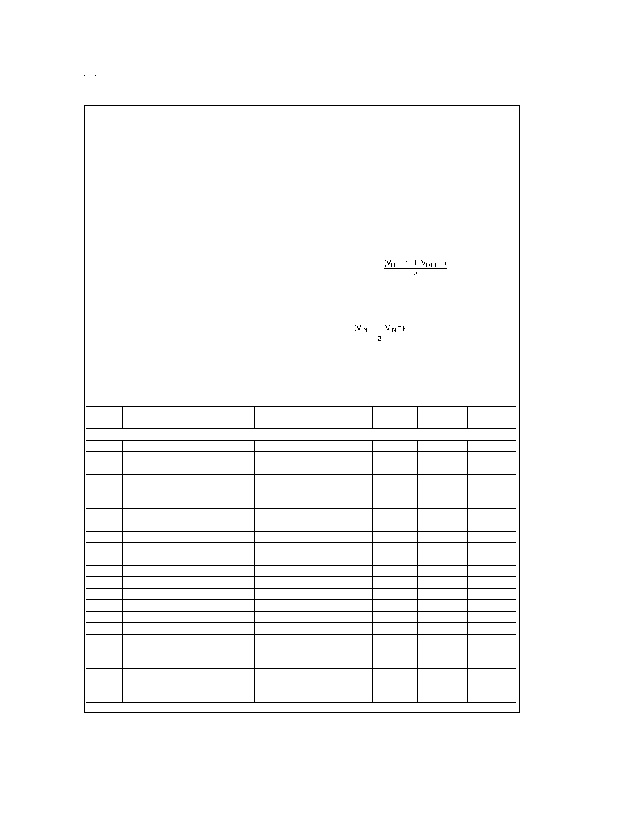
Converter Electrical Characteristics
The following specifications apply for V
+
= V
A
+ = V
D
+ = +3.3 V
DC
, V
REF
+ = +2.500 V
DC
, V
REF
- = 0 V
DC
, 12-bit + sign conver-
sion mode, f
CK
= f
SK
= 5 MHz, R
S
= 25
, source impedance for V
REF
+ and V
REF
-
25
, fully-differential input with fixed
1.250V common-mode voltage, and 10(t
CK
) acquisition time unless otherwise specified. Boldface limits apply for T
A
= T
J
=
T
MIN
to T
MAX
; all other limits T
A
= T
J
= 25∞C. (Notes 7, 8, 9)
Symbol
Parameter
Conditions
Typical
(Note 10)
Limits
Units
(Limits)
(Note 11)
STATIC CONVERTER CHARACTERISTICS
Resolution with No Missing Codes
12 + sign
Bits (min)
+ILE
Positive Integral Linearity Error
After Auto-Cal (Notes 12, 18)
±
1/2
±
1
LSB (max)
-ILE
Negative Integral Linearity Error
After Auto-Cal (Notes 12, 18)
±
1/2
±
1
LSB (max)
DNL
Differential Non-Linearity
After Auto-Cal
±
1
LSB (max)
Positive Full-Scale Error
After Auto-Cal (Notes 12, 18)
±
1/2
±
2
LSB (max)
Negative Full-Scale Error
After Auto-Cal (Notes 12, 18)
±
1/2
±
2
LSB (max)
Offset Error
After Auto-Cal (Notes 5, 18)
±
1/2
±
2
LSB (max)
V
IN
(+) = V
IN
(-) = 1.250V
DC Common Mode Error
After Auto-Cal (Note 15)
±
2
±
3.5
LSB (max)
TUE
Total Unadjusted Error
After Auto-Cal
±
1
LSB
(Notes 12, 13, 14)
Resolution with No Missing Codes
8-bit + sign mode
8 + sign
Bits (min)
+INL
Positive Integral Linearity Error
8-bit + sign mode (Note 12)
±
1/2
LSB (max)
-INL
Negative Integral Linearity Error
8-bit + sign mode (Note 12)
±
1/2
LSB (max)
DNL
Differential Non-Linearity
8-bit + sign mode
±
3/4
LSB (max)
Positive Full-Scale Error
8-bit + sign mode (Note 12)
±
1/2
LSB (max)
Negative Full-Scale Error
8-bit + sign mode (Note 12)
±
1/2
LSB (max)
Offset Error
8-bit + sign mode,
after Auto-Zero (Note 13)
±
1/2
LSB (max)
V
IN
(+) = V
IN
(-) = + 1.250V
TUE
Total Unadjusted Error
8-bit + sign mode
after Auto-Zero
±
3/4
LSB (max)
(Notes 12, 13, 14)
www.national.com
5