TL H 11454
ADC16071ADC16471
16-Bit
Delta-Sigma
192
kss
Analog-to-Digital
Converters
February 1995
ADC16071 ADC16471
16-Bit Delta-Sigma 192 ks s Analog-to-Digital Converters
General Description
The ADC16071 ADC16471 are 16-bit delta-sigma analog-
to-digital
converters
using
64
c
oversampling
at
12 288 MHz A 5th-order comb filter and a 246 tap FIR deci-
mation filter are used to achieve an output data rate of up to
192 kHz The combination of oversampling and internal digi-
tal filtering greatly reduces the external anti-alias filter re-
quirements to a simple RC low pass filter The FIR filters
offer linear phase response 0 005 dB passband ripple and
t
90 dB stopband rejection The ADC16071 ADC16471's
analog fourth-order modulator uses switched capacitor
technology A built-in fully-differential bandgap voltage ref-
erence is also included in the ADC16471 The ADC16071
has no internal reference and requires externally applied
reference voltages
The ADC16071 ADC16471 use an advanced BiCMOS pro-
cess for a low power consumption of 500 mW (max) while
operating from a single 5V supply A power-down mode re-
duces the power supply current from 100 mA (max) in the
active mode to 1 3 mA (max)
The ADC16071 ADC16471 are ideal analog-to-digital front
ends for signal processing applications They provide a
complete high resolution signal acquisition system that re-
quires a minimal external anti-aliasing filter reference or
interface logic
The ADC16071 ADC16471's serial interface is compatible
with the DSP56001 TMS320 and ADSP2100 digital signal
processors
Key Specifications
Y
Resolution
16 bits
Y
Total harmonic distortion
48 kHz output data rate
b
94 dB (typ)
192 kHz output data rate
b
80 dB (typ)
Y
Maximum output data rate
192 kHz (min)
Y
Power dissipation
Active
192 kHz output data rate
500 mW (max)
48 kHz output data rate
275 mW (max)
Power-down
6 5 mW (max)
Key Features
Y
Voltage reference (ADC16471 only)
Y
Fourth-order modulator
Y
64
c
oversampling with a 12 288 MHz sample rate
Y
Adjustable output data rate from 7 kHz to 192 kHz
Y
Linear-phase digital anti-aliasing filter
0 005 dB passband ripple
90 dB stopband rejection
Y
Single
a
5V supply
Y
Power-down mode
Y
Serial data interface compatible with popular
DSP devices
Applications
Y
Medical instrumentation
Y
Process control systems
Y
Test equipment
Y
High sample-rate audio
Y
Digital Signal Processing (DSP) analog front-end
Y
Vibration and noise analysis
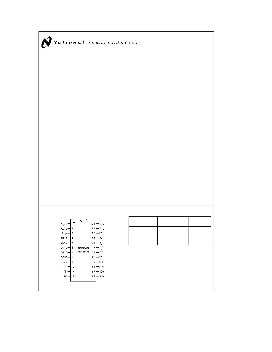
Connection Diagram
TL H 11454 � 2
Ordering Information
Part No
Package
NS Package
No
ADC16471CIN
24-Pin Molded DIP
N24C
ADC16471CIWM
24-Pin SOIC
M24B
ADC16071CIN
24-Pin Molded DIP
N24C
ADC16071CIWM
24-Pin SOIC
M24B
TRI-STATE
is a registered trademark of National Semiconductor Corporation
C1995 National Semiconductor Corporation
RRD-B30M75 Printed in U S A
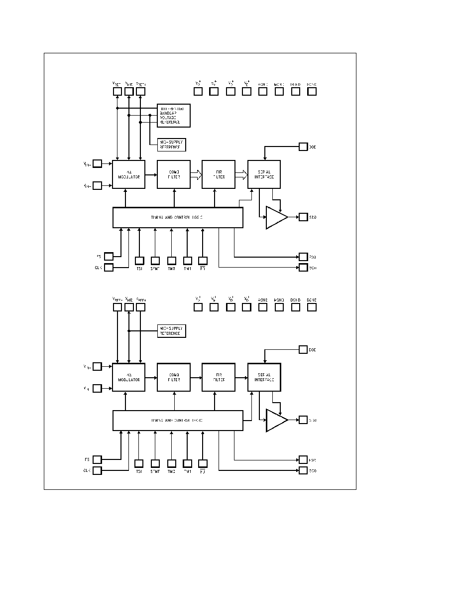
Block Diagram
ADC16471
TL H 11454 � 1
ADC16071
TL H 11454 � 22
2

Absolute Maximum Ratings
(Notes 1 and 2)
If Military Aerospace specified devices are required
please contact the National Semiconductor Sales
Office Distributors for availability and specifications
Supply Voltage (V
A
a
V
D
a
and V
M
a
)
a
6 5V
Logic Control Inputs
b
0 3V to V
D
a
a
0 3V
Voltage at Other
Inputs and Outputs
b
0 3V to V
A
a
e
V
M
a
a
0 3V
Input Current at Any Pin (Note 3)
g
25 mA
Package Input Current (Note 3)
g
100 mA
Maximum Junction Temperature (Note 4)
150 C
Storage Temperature
b
65 C to
a
150 C
Lead Temperature
N Package (Soldering 10 sec )
300 C
WM Package (Infrared 15 sec )
220 C
WM Package (Vapor Phase 60 sec )
215 C
ESD Susceptibility (Note 5)
Human Body Model
4000V
Machine Model
250V
See AN-450 ``Surface Mounting Methods and Their Effect
on Product Reliability'' for other methods of soldering sur-
face mount devices
Operating Ratings
(Notes 1 and 2)
Temperature Range
(T
min
s
T
A
s
T
max
)
ADC16471CIN ADC16071CIN
b
40 C
s
T
A
s
a
85 C
ADC16471CIWM ADC16071CIWM
Supply Voltage
V
A
a
V
D
a
V
M
a
4 75V to 5 25V
Converter Electrical Characteristics
The following specifications apply for V
M
a
e
V
A
a
e
V
D
a
e
5 0V
DC
V
MID
e
V
A
a
2
e
2 50V V
REFa
e
V
MID
a
1 25V
V
REFb
e
V
MID
b
1 25V f
CLK
e
24 576 MHz and dynamic tests are performed with an input signal magnitude set at
b
6 dB
with respect to a full-scale input unless otherwise specified Boldface limits apply for T
A
e
T
J
e
T
min
to T
max
all other
limits T
A
e
T
J
e
25 C
Symbol
Parameter
Conditions
Typical
Limits
Units
(Note 6)
(Note 7)
(Limit)
Resolution
16
Bits
f
CLK
e
24 576 MHz (f
s
e
192 kHz)
S (N
a
D)
Signal-to-Noise
a
Distortion Ratio
Measurement bandwidth
e
0 45f
s
76
72
dB (min)
f
IN
e
19 kHz
THD
Total Harmonic Distortion
f
IN
e
19 kHz
0 010
0 022
% (max)
IMD
Intermodulation Distortion
f
1
e
18 5 kHz f
2
e
19 5 kHz
0 010
0 017
% (max)
Converter Noise Floor (Note 8)
Measurement Bandwidth
e
0 45f
s
b
88
b
77
dBFS (min)
f
CLK
e
6 144 MHz (f
s
e
48 kHz)
S (N
a
D)
Signal-to-Noise
a
Distortion Ratio
Measurement bandwidth
e
0 45f
s
85
80
dB (min)
f
IN
e
5 kHz
73
dB (min)
THD
Total Harmonic Distortion
f
IN
e
5 kHz
0 002
0 0055
% (max)
0 008
% (max)
IMD
Intermodulation Distortion
f
1
e
4 kHz f
2
e
5 5 kHz
0 003
0 009
% (max)
0 01
% (max)
Converter Noise Floor (Note 8)
Measurement Bandwidth
e
0 45f
s
b
99
b
92
dBFS (min)
b
89
dBFS (min)
OTHER CONVERTER CHARACTERISTICS
Z
IN
Input Impedance (Note 9)
34
kX
D
A
V
Gain Error
g
0 2
g
1 0
%FS (max)
V
OS
Input Offset Voltage
15
mV
I
A
Analog Power Supply Current
23
31
mA (max)
I
M
Modulator Power Supply Current
f
CLK
e
24 576 MHz
1 6
2 4
mA (max)
f
CLK
e
6 144 MHz
0 4
0 8
I
D
Digital Power Supply Current
f
CLK
e
24 576 MHz
50
65
mA (max)
f
CLK
e
6 144 MHz
13
23
I
SPD
Power-Down Supply Current
I
A
a
I
D
a
I
M
0 25
1 3
mA
P
D
Power Dissipation
0 375
0 5
W
V
MID
V
A
a
2
V
3
Digital Filter Characteristics
The following specifications apply for V
A
a
e
V
D
a
e
V
M
a
e
5V unless otherwise specified Boldface limits apply for
T
A
e
T
J
e
T
min
to T
max
all other limits T
A
e
T
J
e
25 C
Symbol
Parameter
Conditions
Typical
Limits
Units
(Note 6)
(Note 7)
(Limit)
Stopband Rejection
b
90 0
dB
Passband Ripple
g
0 005
dB
3 dB Cutoff Frequency
0 45
fs
Data Latency
3 968
Clock Cycles
Reference Characteristics
(ADC16471 Only)
The following specifications apply for V
A
a
e
V
D
a
e
V
M
a
e
5V unless otherwise specified Boldface limits apply for T
A
e
T
J
e
T
min
to T
max
all other limits T
A
e
T
J
e
25 C
Symbol
Parameter
Conditions
Typical
Limits
Units
(Note 6)
(Note 7)
(Limit)
V
REF
a
Positive Internal Reference
V
MID
a
1 25
V
MID
a
1 175
V (min)
Output Voltage
V
MID
a
1 325
V (max)
V
REF
b
Negative Internal Reference
V
MID
b
1 25
V
MID
b
1 325
V (min)
Output Voltage
V
MID
b
1 175
V (max)
D
(V
REFa
�
Internal Reference
30
ppm C
V
REFb
) DT
Temperature Coefficient
D
V
REFa
D
I
Positive Internal Reference
Sourcing (0 mA
s
I
s
a
10 mA)
3 4
6 0
Load Regulation
Sinking (
b
1 mA
s
I
s
0 mA)
mV (max)
D
V
REFb
D
I
Negative Internal Reference
Sinking (
b
1 mA
s
I
s
0 mA)
3 2
6 0
Load Regulation
Sourcing (0 mA
s
I
s
10 mA)
Input Reference Characteristics
(ADC16071 Only)
The following specifications apply for V
A
a
e
V
D
a
e
V
M
a
e
5V
Symbol
Parameter
Conditions
Typical
Limits
Units
(Note 6)
(Note 7)
V
REFa
Positive Reference Voltage
1
V
V
A
a
V
V
REFb
Negative Reference Voltage
0
V
V
A
a b
1
V
V
REFa
� V
REFb
Total Reference Voltage
1
V
V
A
a
V
4
DC Electrical Characteristics
The following specifications apply for V
A
a
e
V
D
a
e
V
M
a
e
5V unless otherwise specified Boldface limits apply for T
A
e
T
J
e
T
MIN
to T
MAX
all other limits T
A
e
T
J
e
25 C
Symbol
Parameter
Conditions
Typical
Limits
Units
(Note 6)
(Note 7)
(Limit)
V
IH
Logic High Input Voltage
V
D
a
e
5 25V
V
D
a
V (max)
2 3
V (min)
V
IL
Logic Low Input Voltage
V
D
a
e
4 75V
0 8
V (max)
b
0 3
V (min)
V
OH
Logic High Output Voltage
Logic High Output Current
e b
400 mA
2 4
V (min)
V
D
a
e
4 75V
V
OL
Logic Low Output Voltage
Logic Low Output Current
e
2 mA
0 5
V (max)
V
D
a
e
5 25V
I
IN(1)
Logical ``1'' Input Current
1 0
5 0
m
A (max)
I
IN(0)
Logical ``0'' Input Current
b
1 0
b
5 0
m
A (max)
I
TSI
SDO TRI-STATE Leakage Current
V
IN
e
0 4V to 2 4V
1 0
5 0
m
A (max)
C
IN
Logic Input Capacitance
V
IN
e
0 to V
D
a
5
pF
AC Electrical Characteristics for Clock In (CLK) Serial Clock Out (SCO) and
Frame Sync In (FSI)
The following specifications apply for V
A
a
e
V
D
a
e
V
M
a
e
5V unless otherwise specified Boldface limits apply for T
A
e
T
J
e
T
MIN
to T
MAX
all other limits T
A
e
T
J
e
25 C
Symbol
Parameter
Conditions
Typical
Limits
Units
(Note 6)
(Note 7)
(Limit)
f
CLK
CLK Frequency Range
25
MHz (max)
(f
CLK
e
1 t
CLK
)
1
MHz (min)
t
CLK
CLK Period
1000
ns (max)
(t
CLK
e
1 f
CLK
)
40
ns (min)
t
CLKL
CLK Low Pulse Width
16
ns (min)
t
CLKH
CLK High Pulse Width
14
ns (min)
t
R
CLK Rise Time
10
ns (max)
3
ns (min)
t
F
CLK Fall Time
10
ns (max)
3
ns (min)
t
FSILOW
Minimum Frame Sync Input
2
t
CLK
(min)
Low Time before Frame Sync
Input Asserted High
t
FSISU
Frame Sync Input Setup Time
10
ns (min)
t
FSIH
Frame Sync Input Hold Time
10
ns (min)
t
SCOD
Serial Clock Output Delay
20
ns (max)
Time from Rising Edge
12
5
ns (min)
of CLK
t
SCO
Serial Clock Output Period
4
t
CLK
5