
ADCV0831
8 Bit Serial I/O Low Voltage Low Power ADC with
Auto Shutdown in a SOT Package
General Description
The ADCV0831 is a low voltage 8-bit successive approxima-
tion A/D converter with serial I/O. The I/O is a 3-wire serial in-
terface compatible with NSC's MICROWIRE
TM
& Motorola's
SPI standards. It easily interfaces with standard shift regis-
ters or microprocessors.
Low voltage and auto shutdown features make the
ADCV0831 ideal for portable battery operated electronic de-
vices. The main benefits are most apparent in small portable
electronic devices. The tiny A/D converter can be placed
anywhere on the board.
Applications
n
Digitizing automotive sensors
n
Process control monitoring
n
Remote sensing in noisy environments
n
Instrumentation
n
Test systems
n
Embedded diagnostics
Features
n
Tiny 6-pin SOT 23 package
n
Serial digital data link requires few I/O pins
n
Auto Shutdown
n
0V to 3V analog input range with single 3V power
supply
n
TTL/CMOS input/output compatible
Key Specifications
(For 3V supply, typical, unless otherwise noted.)
n
Resolution:
8 bits
n
Conversion time (f
C
= 700 kHz):
16µs
n
Low power dissipation:
720µW
n
Single supply:
2.7V to 5V
DC
n
Linearity error:
±
1.5LSB over temperature
n
No missing codes over temperature
n
Shutdown supply current 10nA
Ordering Information
Temperature Range
(0∞C
T
j
+70∞C)
Package
Supplied As
ADCV0831M6
MA06A
1k Units Tape and Reel
ADCV0831M6X
MA06A
3k Units Tape and Reel
Connection Diagram
TRI-STATE
Æ
is a registered trademark of National Semiconductor Corporation.
COPS
TM
microcontrollers and MICROWIRE
TM
are trademarks of National Semiconductor Corporation.
ADCV0831
DS100104-1
February 2000
ADCV0831
8
Bit
Serial
I/O
Low
V
oltage
Low
Power
ADC
with
Auto
Shutdown
in
a
SOT
Package
© 2000 National Semiconductor Corporation
DS100104
www.national.com
Absolute Maximum Ratings
(Notes 1, 3)
If Military/Aerospace specified devices are required,
please contact the National Semiconductor Sales Office/
Distributors for availability and specifications.
Supply Voltage (V
CC
)
5.5V
Voltage at Inputs and Outputs
-0.3V to V
CC
+ 0.3V
Input Current at Any Pin (Note 4)
±
5 mA
Package Input Current (Note 4)
±
20 mA
Power Dissipation at T
A
= 25∞C
(Note 5)
470 mW
ESD Susceptibility (Note 6)
2000V
Soldering Temperature (Note 7)
Convection Infrared (15 sec.)
215∞C
Wave Soldering (4 sec.) (Note 7)
260∞C
Storage Temperature
-65∞C to +150∞C
Thermal Resistance (
JA
)
265∞C/W
Operating Ratings
(Notes 2, 3)
Temperature Range
0∞C
T
j
70∞C
Supply Voltage (V
CC
)
2.7V
DC
to 5V
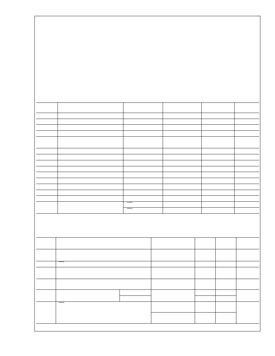
Electrical Characteristics
The following specifications apply for V
CC
= 3V
DC
, and f
CLK
= 500 kHz unless otherwise specified. Boldface limits apply for
T
A
= T
J
= T
MIN
to T
MAX
; all other limits T
A
= T
J
= 25∞C.
Symbol
Parameter
Conditions
Typical
(Note 8)
Limits
(Note 9)
Units
Integral Linearity Error
±
0.6
±
1.5
LSB (max)
Offset Error
±
0.1
±
1.5
LSB (max)
Full Scale Error
±
0.3
±
1.5
LSB (max)
Resolution
8
Bits (min)
V
IN
Analog Input Voltage
(V
CC
+ 0.05)
V (max)
(GND - 0.05)
V (min)
V
IN(1)
Logical "1" Input Voltage
V
CC
= 3V
2.0
V (min)
V
IN(0)
Logical "0" Input Voltage
V
CC
= 3V
0.8
V (max)
I
IN(1)
Logical "1" Input Current
V
IN
= 3V
0.01
1
µA (max)
I
IN(0)
Logical "0" Input Current
V
IN
= 0V
0.01
-1
µA (max)
V
OUT(1)
Logical "1" Output Voltage
I
out
=-360µA
2.8
2.4
V (min)
V
OUT(0)
Logical "0" Output Voltage
I
out
=1.6 mA
0.24
0.4
V (max)
I
OUT
TRI-STATE
Æ
Output Current
V
OUT
= 0V
0.01
3.0
µA (max)
I
SOURCE
Output Source Current
V
OUT
= 0V
2.6
1.0
mA (min)
I
SINK
Output Sink Current
V
OUT
= 3V
7.4
3.0
mA (min)
I
CC
Supply Current
CS = HIGH
0.01
30
µA (max)
CS = LOW
200
400
µA (max)
AC Electrical Characteristics
The following specifications apply for V
CC
= +3 V
DC
, and t
r
= t
f
= 20 ns unless otherwise specified. Boldface limits apply for
T
A
= T
J
= T
MIN
to T
MAX
; all other limits T
A
= T
J
= 25∞C.
Symbol
Parameter
Conditions
Typical
Limits
Units
(Note 8)
(Note 9)
f
CLK
Clock Frequency
700
kHz (max)
10
kHz (min)
t
SET-UP
CS failing edge to CLK rising edge
25
ns
Clock Duty Cycle
40
% (min)
60
% (max)
T
C
Conversion Time
11
Clock
Periods
t
pd
CLK Falling Edge to Data Valid
Low to High
C
L
= 100 pF
142
250
ns (max)
High to Low
70
200
t
1H
, t
0H
CS Rising Edge to Data Output TRI-STATE
C
L
= 100 pF, R
L
=2
k
75
250
ns (max)
(see TRI-STATE Test Circuits)
C
L
= 100 pF, R
L
= 10
k
50
ADCV0831
www.national.com
2
AC Electrical Characteristics
(Continued)
The following specifications apply for V
CC
= +3 V
DC
, and t
r
= t
f
= 20 ns unless otherwise specified. Boldface limits apply for
T
A
= T
J
= T
MIN
to T
MAX
; all other limits T
A
= T
J
= 25∞C.
Symbol
Parameter
Conditions
Typical
Limits
Units
(Note 8)
(Note 9)
C
IN
Capacitance of Logic Inputs
5
pF
C
OUT
Capacitance of Logic Outputs
5
pF
Note 1: Absolute Maximum Ratings indicate limits beyond which damage to the device may occur.
Note 2: Operating Ratings indicate conditions for which the device is functional. These ratings do not guarantee specific performance limits. For guaranteed speci-
fications and test conditions, see the Electrical Characteristics. The guaranteed specifications apply only for the test conditions listed. Some performance character-
istics may degrade when the device is not operated under the listed test conditions.
Note 3: All voltages are measured with respect to GND = 0 V
DC
, unless otherwise specified.
Note 4: When the input voltage V
IN
at any pin exceeds the power supplies (V
IN
<
GND or V
IN
>
V
CC
) the current at that pin should be limited to 5 mA. The 20 mA
maximum package input current rating limits the number of pins that can safely exceed the power supplies with an input current of 5 mA to four pins.
Note 5: The maximum power dissipation must be derated at elevated temperatures and is dictated by T
JMAX
,
JA
and the ambient temperature, T
A
. The maximum
allowable power dissipation at any temperature is P
D
= (T
JMAX
- T
A
)/
JA
or the number given in the Absolute Maximum Ratings, whichever is lower.
Note 6: Human body model, 100 pF capacitor discharged through a 1.5 k
resistor.
Note 7: See AN450 "Surface Mounting Methods and Their Effect on Product Reliability" or Linear Data Book section "Surface Mount" for other methods of soldering
surface mount devices.
Note 8: Typicals are at T
J
= 25∞C and represent the most likely parametric norm.
Note 9: Guaranteed to National's AOQL (Average Outgoing Quality Level).
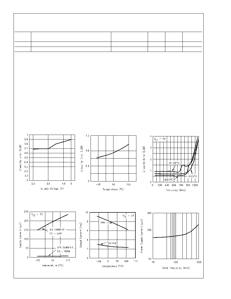
Typical Performance Characteristics
The following specifications apply for V
CC
= 3V, unless otherwise specified
Integral Linearity Error vs
Supply Voltage
DS100104-62
Linearity Error vs
Temperature
DS100104-56
Linearity Error vs
Clock Frequency
DS100104-55
Power Supply Current
vs Temperature
DS100104-57
Output Current vs
Temperature
DS100104-58
Power Supply Current
vs Clock Frequency
DS100104-61
ADCV0831
www.national.com
3

TRI-STATE Test Circuits and Waveforms
Timing Diagrams
DS100104-8
Data Output Timing
DS100104-10
Start Conversion Timing
DS100104-11
ADCV0831
www.national.com
4

Timing Diagrams
(Continued)
Timing
DS100104-12
ADCV0831
www.national.com
5