 | –≠–ª–µ–∫—Ç—Ä–æ–Ω–Ω—ã–π –∫–æ–º–ø–æ–Ω–µ–Ω—Ç: AN-242 | –°–∫–∞—á–∞—Ç—å:  PDF PDF  ZIP ZIP |
TL H 7479
Applying
a
New
Precision
Op
Amp
AN-242
National Semiconductor
Application Note 242
April 1980
Applying a New
Precision Op Amp
Robert J Widlar
Apartado Postal 541
Puerto Vallarta Jalisco
Mexico
Bob Pease and Mineo Yamatake
National Semiconductor Corporation
Santa Clara California
U S A
Abstract
A new bipolar op amp design has advanced the
state of the art by reducing offset voltage and bias current
errors Its characteristics are described here indicating an
ultimate input resolution of 10 mV and 1 pA under laboratory
conditions Practical circuits for making voltmeters amme-
ters differential instrumentation amplifiers and a variety of
other designs that can benefit from the improved perform-
ance are covered in detail Methods of coupling the new
device to existing fast amplifiers to take advantage of the
best characteristics of both even in follower applications
are explored
introduction
A low cost mass-produced op amp with electrometer-type
input currents combined with low offset voltage and drift is
now available Designated the LM11 this IC can minimize
production problems by providing accuracy without adjust-
ments even in high-impedance circuitry On the other hand
if pushed to its full potential what has been impossible in
the past becomes entirely practical
Significantly the LM11 is not restricted to commercial and
industrial use Devices can be completely specified over a
b
55 C to
a
125 C range Preliminary data indicates that
reliability is the same as standard ICs qualified for military
and space applications
The essential details of the design along with an introduc-
tion to the peculiarities of high-impedance circuits have
been presented elsewhere
This will be expanded here
Practical circuitry that reduces effective bias current for
those applications where performance cannot be made de-
pendent on offset current are described In addition circuits
combining the DC characteristics of the new part with the
AC performance of existing fast amplifiers will be shown
This will be capped with a number of practical designs to
provide some perspective into what might be done
dc errors
Barring the use of chopper or reset stabilization the best
offset voltage drift and long-term stability are obtained us-
ing bipolar transistors for the op amp input stage This has
been done with the LM11 On-wafer trimming further im-
proves performance
Typically
a 100 mV offset with
1 mV C drift results
Transistors with typical current gains of 5000 have been
used in the manufacture of the LM11 The input stage em-
ploys a Darlington connection that has been modified so
that offset voltage and drift are not degraded The typical
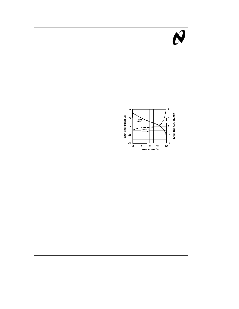
input currents plotted in
Figure 1 demonstrate the value of
the approach
TL H 7479 ≠ 1
Figure 1 Below 100 C bias current varies almost linear-
ly with temperature This means that simple
circuitry can be used for compensation Offset
current is unusually low
The offset current of this op amp is so low that it cannot be
measured on existing production test equipment Therefore
it probably cannot be specified tighter than 10 pA For crit-
ical applications the user should have little difficulty in se-
lecting to a tighter limit
The bias current of the LM11 equals that of monolithic FET
amplifier at 25 C Unlike FETs it does not double every
10 C In fact the drift over a
b
55 C to
a
125 C temperature
range is about the same as that of a FET op amp during
normal warm up
Other characteristics are summarized in Table I It can be
seen that the common-mode rejection supply-voltage re-
jection and voltage gain are high enough to take full advan-
tage of the low offset voltage The unspectacular 0 3V ms
slew rate is balanced by the 300 mA current drain
R J Widlar ``Working with High Impedance Op Amps'' National Semiconductor AN-241
C1995 National Semiconductor Corporation
RRD-B30M115 Printed in U S A
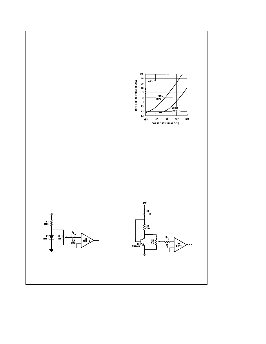
Table I Typical characteristics of the
LM11 for T
j
e
25 C and V
S
e
g
15V Operation is
specified down to V
S
e
g
2 5V
Parameter
Conditions
Value
Input Offset Voltage
100 mV
Input Offset Current
500 fA
Input Bias Current
25 pA
Input Noise Voltage 0 01 Hz
s
f
s
10 Hz
8 mVpp
Input Noise Current 0 01 Hz
s
f
s
10 Hz
1 pApp
Long Term Stability T
j
e
25 C
10 mV
Offset Voltage Drift
b
55 C
s
T
j
s
125 C
1 mV C
Offset Current Drift
b
55 C
s
T
j
s
125 C
20 fA C
Bias Current Drift
b
55 C
s
T
j
s
125 C
500 fA C
Voltage Gain
V
OUT
e
g
12V
1 200V mV
I
OUT
e
g
0 5 mA
V
OUT
e
g
12V
300V mV
I
OUT
e
g
2 mA
Common-Mode
b
12 5V
s
V
CM
s
14V
130 dB
Rejection
Supply-Voltage
g
2 5V
s
V
S
s g
20V
118 dB
Rejection
Slew Rate
0 3V ms
Supply Current
300 mA
As might be expected the low bias currents were obtained
with some sacrifice in noise But the low frequency noise
voltage is still a bit less than a FET amplifier and probably
more predictable The latter is important because this noise
cannot be tested in production Long term measurements
have not indicated any drift in excess of the noise This is
not the case for FETs
It is worthwhile noting that the drift of offset voltage and
current is low enough that DC accuracy is noise limited in
room-temperature applications
bias current compensation
The LM11 can operate from MX source resistances with
little increase in the equivalent offset voltage as can be
seen in
Figure 2 This is impressive considering the low ini-
tial offset voltage The situation is much improved if the de-
sign can be configured so that the op amp sees equal resist-
ance on the two inputs However this cannot be done with
all circuits Examples are integrators sample and holds log-
arithmic converters and signal-conditioning amplifiers And
even though the LM11 bias current is low there will be
those applications where it needs to be lower
Referring back to
Figure 1 it can be seen that the bias
current drift is essentially linear over a
b
50 C to
a
100 C
range This is a deliberate consequence of the input stage
design Because of it relatively simple circuitry can be used
to develop a compensating current
TL H 7479 ≠ 2
Figure 2 The LM11 operates from MX source resistanc-
es with little DC error With equal source re-
sistances accuracy is essentially limited by
low frequency current noise
Bias current compensation is not new but making it effec-
tive with even limited temperature excursions has been a
problem An early circuit suggested for bipolar ICs is shown
in
Figure 3a The compensating current is determined by the
diode voltage This does not vary as rapidly with tempera-
ture as bias current nor does it match the usual non-lineari-
ties
With the improved circuit in
Figure 3b the temperature coef-
ficient can be increased by using a transistor and including
R2 The drop across R2 is nearly constant with temperature
The voltage delivered to the potentiometer has a 2 2 mV C
drift while its magnitude is determined by R2 Thus as long
as the bias current varies linearly with temperature a value
for R2 can be found to effect compensation
TL H 7479 ≠ 3
a original circuit
TL H 7479 ≠ 4
b improved version
Figure 3 Bias-current compensation With the improved version the temperature coefficient of the compensating
current can be varied with R2 It is effective only if bias current has linear negative temperature coefficient
2
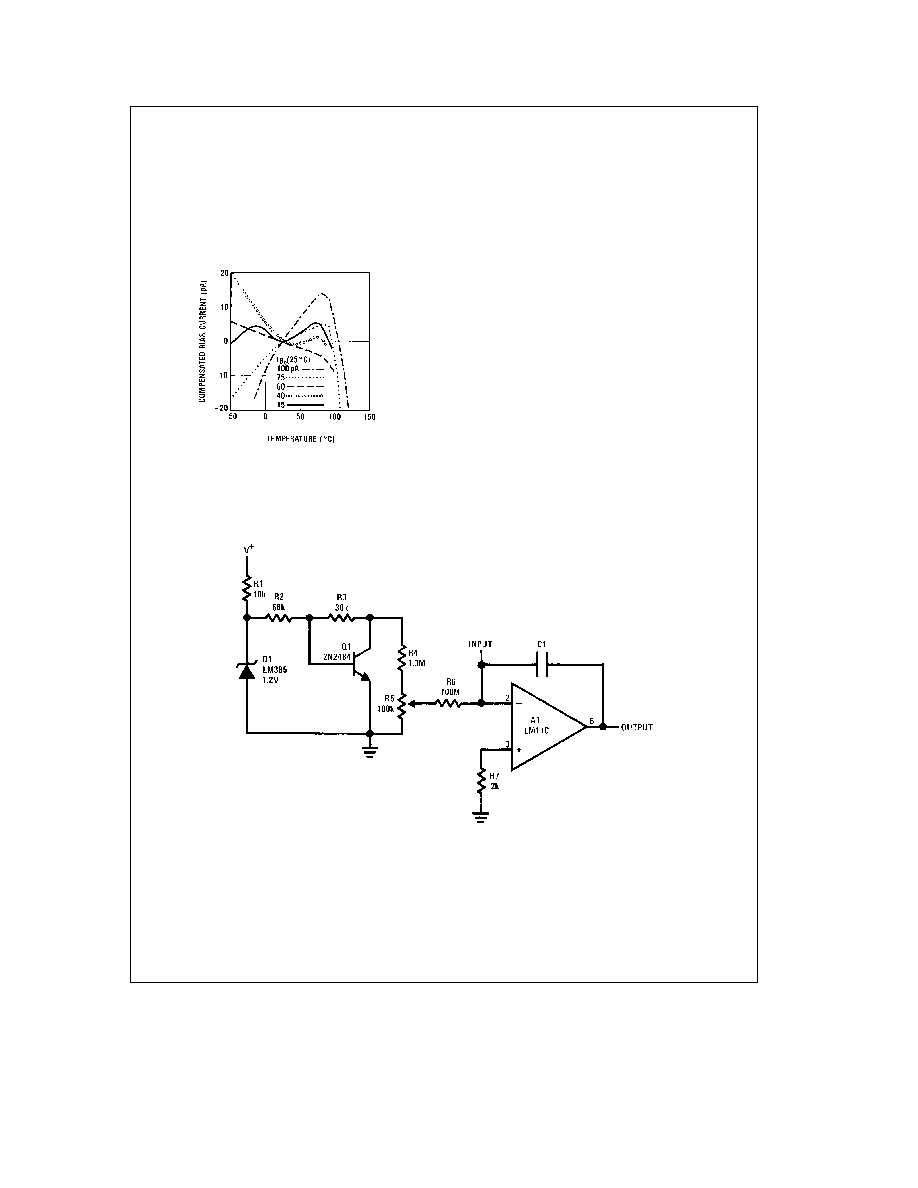
In production altering resistors based on temperature test-
ing is to be avoided if at all possible Therefore the results
that can be obtained with simple nulling at room tempera-
ture and a fixed value for R2 are of interest
Figure 4 gives
this data for a range of parts with different initial bias cur-
rents This was obtained from pre-production and initial-pro-
duction runs The bias current variations were the result of
both h
FE
variations and changes in internal operating cur-
rents and represent the worst as well as best obtained
They are therefore considered a realistic estimate of what
would be encountered among various production lots
TL H 7479 ≠ 5
Figure 4 Compensated bias current for five representa-
tive units with a range of initial bias currents
The circuit in
Figure 3b was used with balanc-
ing at 25 C High drift devices could be im-
proved further by altering R2
Little comment need be made on these results except that
the method is sufficiently predictable that another factor of
five reduction in worst case bias current could be made by
altering R2 based on the results of a single temperature run
One disadvantage of the new circuit is that it is more sensi-
tive to supply variations than the old This is no problem if
the supplies are regulated to 1% But with worst regulation it
suffers because with R2 the transistor no longer functions
as a regulator and because much tighter compensation is
obtained
The circuit in
Figure 5 uses pre-regulation to solve this prob-
lem The added reference diode has a low breakdown so
that the minimum operating voltage of the op amp is unre-
stricted Because of the low breakdown the drop across R3
can no longer be considered constant But it will vary linear-
ly with temperature so this is of no consequence The fact
that this reference can be used for other functions should
not be overlooked because a regulated voltage is frequently
required in designs using op amps
In
Figure 5 a divider is used so that the resistor feeding the
compensating current to the op amp can be reduced There
will be an error current developed for any offset voltage
change across R6 This should not be a problem with the
LM11 because of its low offset voltage But for tight com-
pensation mismatch in the temperature characteristics of
R4 and R5 must be considered
TL H 7479 ≠ 6
Figure 5 Bias current compensation for use with unregulated supplies
Reference voltage is available for other circuitry
3
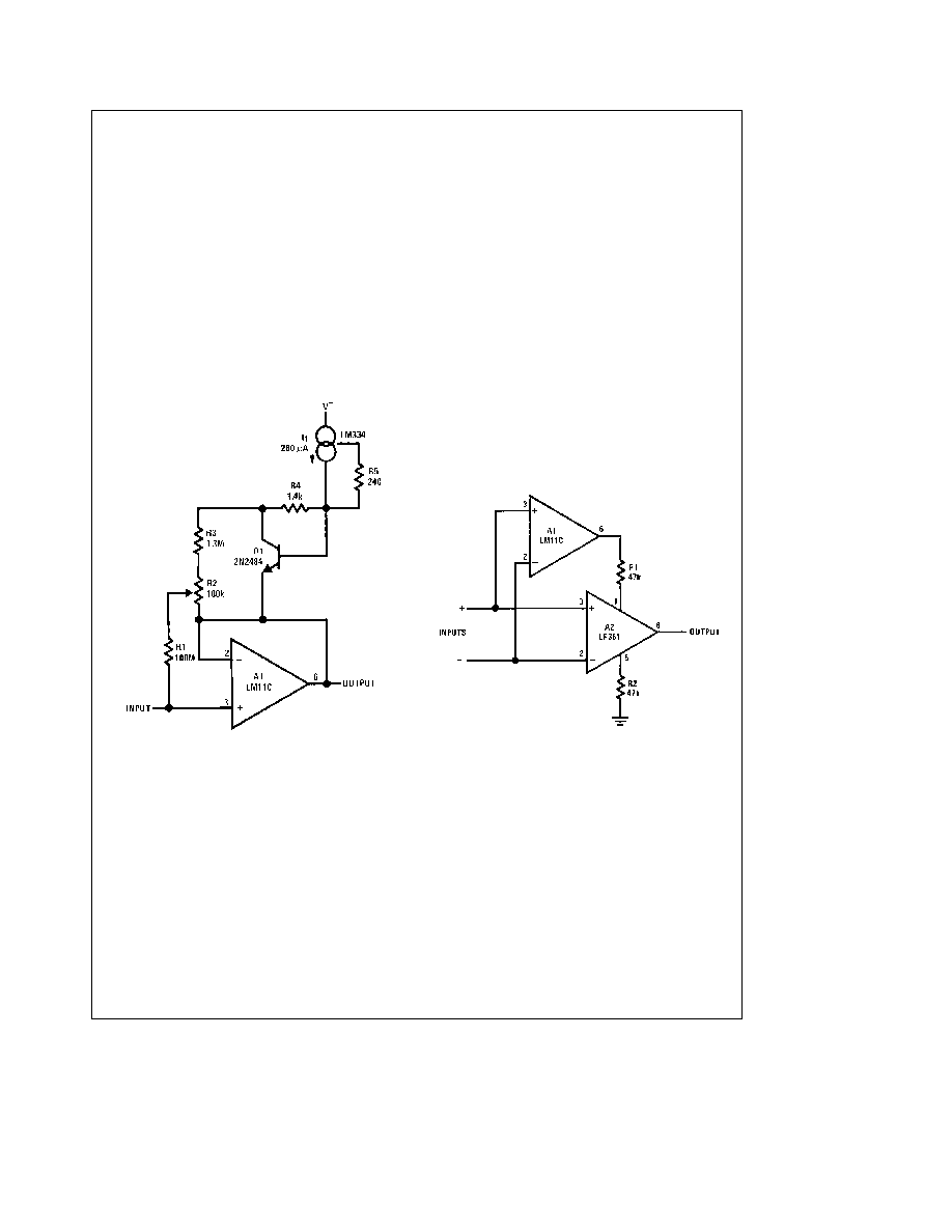
Bias current compensation is more difficult for non-inverting
amplifiers because the common-mode voltage varies With
a voltage follower everything can be bootstrapped to the
output and powered by a regulated current source as
shown in
Figure 6 The LM334 is a temperature sensor It
regulates against voltage changes and its output varies lin-
early with temperature so it fits the bill
Although the LM334 can accommodate voltage changes
fast enough to work with the LM11 it is not fast enough for
the high-speed circuits to be described But compensation
can still be obtained by using the zener diode pre-regulator
bootstrapped to the output and powered by either a resistor
or FET current source The LM385 fits well here because
both the breakdown voltage and minimum operating current
are low
With ordinary op amps the collector base voltage of the
input transistors varies with the common-mode voltage A
50% change in bias current over the common-mode range
is not unusual so compensating the bias current of a follow-
er has limited value However the bootstrapped input stage
of the LM11 reduces this to about 2 pA for a
g
20V com-
mon-mode swing giving a 2
c
10
13
X
common-mode input
resistance
fast amplifiers
A precision DC amplifier although slow can be used to sta-
bilize the offset voltage of a less precise fast amplifier As
shown in
Figure 7 the slow amplifier senses the voltage
across the input terminals and supplies a correction signal
to the balance terminals of the fast amplifier The LM11 is
particularly interesting in this respect as it does not degrade
the input bias current of the composite even when the fast
amplifier has a FET input
Surprisingly with the LM11 this will work for both inverting
and non-inverting connections because its common-mode
slew recovery is a lot faster than that of the main loop This
was accomplished
even with circuitry running under
100 nA by proper clamping and by bootstrapping of internal
stray capacitances
TL H 7479 ≠ 7
Figure 6 This circuit shows how bias current compen-
sation can be used on a voltage follower
TL H 7479 ≠ 8
Figure 7 A slow amplifier can be used to null the offset
of a fast amplifier
4
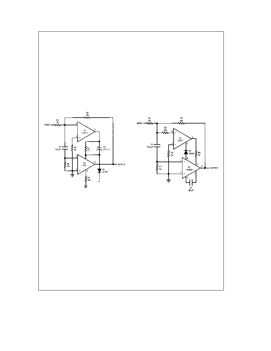
An optimized circuit for the inverting amplifier connection is
shown in
Figure 8 The LM11 is DC coupled to the input and
drives the balance terminals of the fast amplifier The fast
amplifier is AC coupled to the input and drives the output
This isolates FET leakage from the input circuitry
As can be seen the method of coupling into the balance
terminals will vary depending on the internal configuration of
the fast amplifier If the quiescent voltage on the balance
terminals is beyond the output swing of the LM11 a differ-
ential coupling must be used as in
Figure 8a A lead capaci-
tor C2 reduces the AC swing required at the LM11 output
The clamp diode D1 insures that the LM11 does not over-
drive the fast amplifier in slew
If the quiescent voltage on the balance terminals is such
that the LM11 can drive directly the circuit in
Figure 8b can
be used A clamp diode from the other balance terminal to
internal circuitry of the LM11 keeps the output from swing-
ing too far from the null value and a resistor may be re-
quired in series with its output to insure stability
Measurements indicate that the slew rate of the fast amplifi-
er is unimpaired as is the settling time to 1 mV for a 20V
output excursion If the composite amplifier is overdriven so
that the output saturates there will be an added recovery
delay because the coupling capacitor to the fast amplifier
takes on a charge with the summing node off ground
Therefore C1 should be made as small as possible But
going below the values given may introduce gain error
If the bias current of the fast amplifier meets circuit require-
ments it can be direct-coupled to the input In this case
offset voltage is improved not bias current But overload
recovery can be reduced The AC coupling to the fast-ampli-
fier input might best be eliminated for limited-temperature-
range operation
This connection also increases the open-loop gain beyond
that of the LM11 particularly since two-pole compensation
can be effected to reduce AC gain error at moderate fre-
quencies The DC gains measured showed something in
excess of 140 dB
TL H 7479 ≠ 9
a with standard BI-FET
TL H 7479 ≠ 10
b with fast hybrid
Figure 8 These inverters have bias current and offset voltage of LM11 along with speed of the FET op amps Open
loop gain is about 140 dB and settling time to 1 mV about 8 ms Excess overload-recovery delay can be
eliminated by directly coupling the FET amplifier to summing node
5