TL F 5940
CD4002MCD4002C
Dual
4-Input
NOR
Gate
CD4012MCD4012C
Dual
4-Input
NAND
Gate
March 1988
CD4002M CD4002C Dual 4-Input NOR Gate
CD4012M CD4012C Dual 4-Input NAND Gate
General Description
These NOR and NAND gates are monolithic complementa-
ry MOS (CMOS) integrated circuits The N- and P-channel
enhancement mode transistors provide a symmetrical cir-
cuit with output swings essentially equal to the supply volt-
age This results in high noise immunity over a wide supply
voltage range No DC power other than that caused by leak-
age current is consumed during static conditions All inputs
are protected against static discharge and latching condi-
tions
Features
Y
Wide supply voltage range
3 0V to 15V
Y
Low power
10 nW (typ )
Y
High noise immunity
0 45 V
DD
(typ )
Applications
Y
Automotive
Y
Alarm system
Y
Data terminals
Y
Industrial controls
Y
Instrumentation
Y
Remote metering
Y
Medical Electronics
Y
Computers
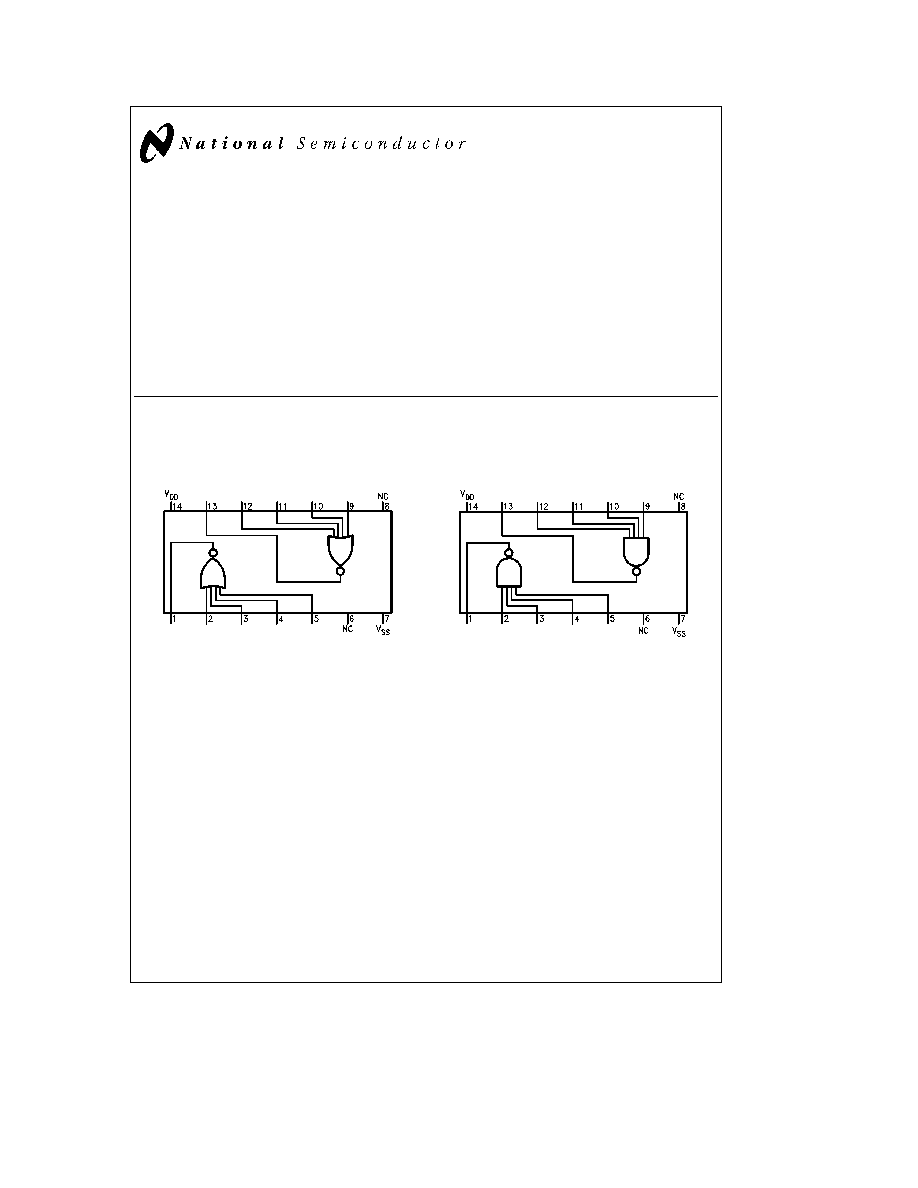
Connection Diagrams
CD4002
Dual-In-Line Package
TL F 5940 � 1
Top View
CD4012
Dual-In-Line Package
TL F 5940 � 2
Top View
Order Number CD4002 or CD4012
C1995 National Semiconductor Corporation
RRD-B30M105 Printed in U S A
Absolute Maximum Ratings
(Note 1)
If Military Aerospace specified devices are required
please contact the National Semiconductor Sales
Office Distributors for availability and specifications
Voltage at Any Pin
V
SS
b
0 3V to V
DD
a
0 3V
Operating Temperature Range
CD4002M CD4012M
b
55 C to
a
125 C
CD4002C CD4012C
b
40 C to
a
85 C
Storage Temperature Range (T
S
)
b
65 C to
a
150 C
Power Dissipation (P
D
)
Dual-In-Line
700 mW
Small Outline
500 mW
Operating Range (V
DD
)
V
SS
a
3 0V to V
SS
a
15V
Lead Temperature (T
L
)
(Soldering 10 seconds)
260 C
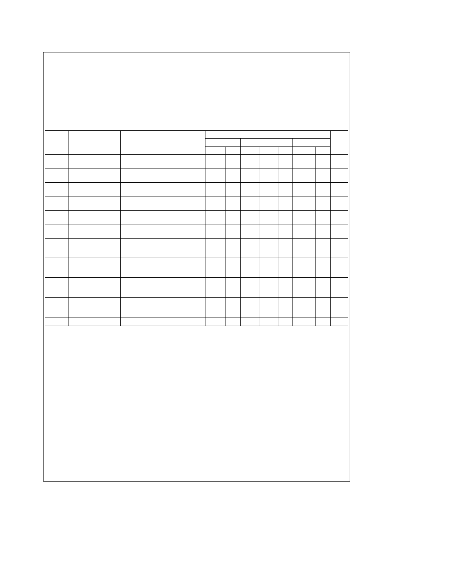
DC Electrical Characteristics
CD4002M CD4012M
Limits
Symbol
Parameter
Conditions
b
55 C
a
25 C
a
125 C
Units
Min
Max
Min
Typ
Max
Min
Max
I
DD
Quiescent
V
DD
e
5 0V
0 05
0 001
0 05
3 0
m
A
Device Current
V
DD
e
10V
0 1
0 001
0 1
6
m
A
P
D
Quiescent Device
V
DD
e
5 0V
0 25
0 005
0 25
15
m
W
Dissipation Package
V
DD
e
10V
1 0
0 01
1 0
60
m
W
V
OL
Output Voltage
V
DD
e
5 0V V
I
e
V
DD
I
O
e
0A
0 05
0
0 05
0 05
V
Low Level
V
DD
e
10V V
I
e
V
DD
I
O
e
0A
0 05
0
0 05
0 05
V
V
OH
Output Voltage
V
DD
e
5 0V V
I
e
V
SS
I
O
e
0A
4 95
4 95
5 0
4 95
V
High Level
V
DD
e
10V V
I
e
V
SS
I
O
e
0A
9 95
9 95
10
9 95
V
V
NL
Noise Immunity
V
DD
e
5 0V V
O
e
3 6V I
O
e
0A
1 5
1 5
2 25
1 4
V
(All Inputs)
V
DD
e
10V V
O
e
7 2V I
O
e
0A
3 0
3 0
4 5
2 9
V
V
NH
Noise Immunity
V
DD
e
5 0V V
O
e
0 95V I
O
e
0A
1 4
1 5
2 25
1 5
V
(All Inputs)
V
DD
e
10V V
O
e
2 9V I
O
e
0A
2 9
3 0
4 5
3 0
V
I
D
N
Output Drive Current
V
DD
e
5 0V V
O
e
0 4V V
I
e
V
DD
0 5
0 40
1 0
0 28
mA
N-Channel (4002)
V
DD
e
10V V
O
e
0 5V V
I
e
V
DD
1 1
0 9
2 5
0 65
mA
(Note 2)
I
D
P
Output Drive Current
V
DD
e
5 0V V
O
e
2 5V V
I
e
V
SS
b
0 62
b
0 5
b
2 0
b
0 35
mA
P-Channel (4002)
V
DD
e
10V V
O
e
9 5V V
I
e
V
SS
b
0 62
b
0 5
b
1 0
b
0 35
mA
(Note 2)
I
D
N
Output Drive Current
V
DD
e
5 0V V
O
e
0 4V V
I
e
V
DD
0 31
0 25
0 5
0 175
mA
N-Channel (4012)
V
DD
e
10V V
O
e
0 5V V
I
e
V
DD
0 63
0 5
0 6
0 35
mA
(Note 2)
I
D
P
Output Drive Current
V
DD
e
5 0V V
O
e
2 5V V
I
e
V
SS
b
0 31
b
0 25
b
0 5
b
0 175
mA
P-Channel (4012)
V
DD
e
10V V
O
e
9 5V V
I
e
V
SS
b
0 75
b
0 6
b
1 2
b
0 4
mA
(Note 2)
I
I
Input Current
10
pA
Note 1
``Absolute Maximum Ratings'' are those values beyond which the safety of the device cannot be guaranteed Except for ``Operating Temperature Range''
they are not meant to imply that the devices should be operated at these limits The table of ``Electrical Characteristics'' provides conditions for actual device
operation
Note 2
I
D
N and I
D
P are tested one output at a time
2

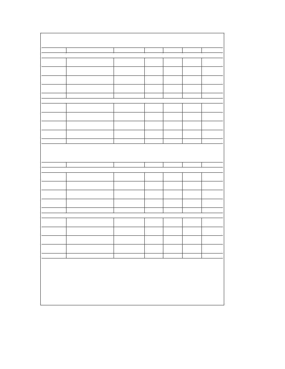
DC Electrical Characteristics
CD4002C CD4012C
Limits
Symbol
Parameter
Conditions
b
55 C
a
25 C
a
85 C
Units
Min
Max
Min
Typ
Max
Min
Max
I
DD
Quiescent
V
DD
e
5 0V
0 5
0 005
0 5
15
m
A
Device Current
V
DD
e
10V
5 0
0 005
5 0
30
m
A
P
D
Quiescent Device
V
DD
e
5 0V
2 5
0 025
2 5
75
m
W
Dissipation Package V
DD
e
10V
50
0 05
50
300
m
W
V
OL
Output Voltage
V
DD
e
5 0V V
I
e
V
DD
I
O
e
0A
0 05
0
0 05
0 05
V
Low Level
V
DD
e
10V V
I
e
V
DD
I
O
e
0A
0 05
0
0 05
0 05
V
V
OH
Output Voltage
V
DD
e
5 0V V
I
e
V
SS
I
O
e
0A
4 95
4 95
5 0
4 95
V
High Level
V
DD
e
10V V
I
e
V
SS
I
O
e
0A
9 95
9 95
10
9 95
V
V
NL
Noise Immunity
V
DD
e
5 0V V
O
t
3 6V I
O
e
0A
1 5
1 5
2 25
1 4
V
(All Inputs)
V
DD
e
10V V
O
t
7 2V I
O
e
0A
3 0
3 0
4 5
2 9
V
V
NH
Noise Immunity
V
DD
e
5 0V V
O
s
0 95V I
O
e
0A
1 4
1 5
2 25
1 5
V
(All Inputs)
V
DD
e
10V V
O
s
2 9V I
O
e
0A
2 9
3 0
4 5
3 0
V
I
D
N
Output Drive Current
V
DD
e
5 0V V
O
e
0 4V V
I
e
V
DD
0 35
0 3
1 0
0 24
mA
N-Channel (4002)
V
DD
e
10V V
O
e
0 5V V
I
e
V
DD
0 72
0 6
2 5
0 48
mA
(Note 2)
I
D
N
Output Drive Current
V
DD
e
5 0V V
O
e
0 4V V
I
e
V
DD
0 145
0 12
0 5
0 095
mA
N-Channel (4012)
V
DD
e
10V V
O
e
0 5V V
I
e
V
DD
0 3
0 25
0 6
0 2
mA
(Note 2)
I
D
P
Output Drive Current
V
DD
e
5 0V V
O
e
2 5V V
I
e
V
SS
b
0 35
b
0 3
b
2 0
b
0 24
mA
P-Channel (4002)
V
DD
e
10V V
O
e
9 5V V
I
e
V
SS
b
0 3
b
0 25
b
1 0
b
0 2
mA
(Note 2)
I
D
P
Output Drive Current
V
DD
e
5 0V V
O
e
2 5V V
I
e
V
SS
b
0 145
b
0 12
b
0 5
b
0 095
mA
P-Channel (4012)
V
DD
e
10V V
O
e
9 5V V
I
e
V
SS
b
0 35
b
0 3
b
1 2
b
0 24
mA
(Note 2)
I
I
Input Current
10
pA
Note 1
``Absolute Maximum Ratings'' are those values beyond which the safety of the device cannot be guaranteed Except for ``Operating Temperature Range''
they are not meant to imply that the devices should be operated at these limits The table of ``Electrical Characteristics'' provides conditions for actual device
operation
Note 2
I
D
N and I
D
P are tested one output at a time
3
AC Electrical Characteristics
T
A
e
25 C C
L
e
15 pF and input rise and fall times
e
20 ns Typical
temperature coefficient for all values of V
DD
e
0 3% C
Symbol
Parameter
Conditions
Min
Typ
Max
Units
CD4002M
t
PHL
Propagation Delay Time
V
DD
e
5 0V
35
50
ns
High to Low Level
V
DD
e
10V
25
40
ns
t
PLH
Propagation Delay Time
V
DD
e
5 0V
35
50
ns
Low to High Level
V
DD
e
10V
25
40
ns
t
THL
Transition Time High
V
DD
e
5 0V
65
175
ns
to Low Level
V
DD
e
10V
35
75
ns
t
TLH
Transition Time Low
V
DD
e
5 0V
65
125
ns
to High Level
V
DD
e
10V
35
70
ns
C
IN
Input Capacitance
Any Input
5 0
pF
CD4002C
t
PHL
Propagation Delay Time
V
DD
e
5 0V
35
120
ns
High to Low Level
V
DD
e
10V
25
65
ns
T
PLH
Propagation Delay Time
V
DD
e
5 0V
35
80
ns
Low to High Level
V
DD
e
10V
25
55
ns
t
THL
Transition Time High
V
DD
e
5 0V
65
300
ns
to Low Level
V
DD
e
10V
35
125
ns
t
TLH
Transition Time Low
V
DD
e
5 0V
65
200
ns
to High Level
V
DD
e
10V
35
115
ns
C
IN
Input Capacitance
Any Input
5 0
pF
AC Parameters are guaranteed by DC correlated testing
AC Electrical Characteristics
T
A
e
25 C C
L
e
15 pF and input rise and fall times
e
20 ns Typical
temperature coefficient for all values of V
DD
e
0 3% C
Symbol
Parameter
Conditions
Min
Typ
Max
Units
CD4012M
t
PHL
Propagation Delay Time
V
DD
e
5 0V
50
75
ns
High to Low Level
V
DD
e
10V
25
40
ns
t
PLH
Propagation Delay Time
V
DD
e
5 0V
50
75
ns
Low to High Level
V
DD
e
10V
25
40
ns
t
THL
Transition Time High
V
DD
e
5 0V
75
125
ns
to Low Level
V
DD
e
10V
50
75
ns
t
TLH
Transition Time Low
V
DD
e
5 0V
75
100
ns
to High Level
V
DD
e
10V
40
60
ns
C
IN
Input Capacitance
Any Input
5 0
pF
CD4012C
t
PHL
Propagation Delay Time
V
DD
e
5 0V
50
100
ns
High to Low Level
V
DD
e
10V
25
50
ns
T
PLH
Propagation Delay Time
V
DD
e
5 0V
50
100
ns
Low to High Level
V
DD
e
10V
25
50
ns
t
THL
Transition Time High
V
DD
e
5 0V
75
150
ns
to Low Level
V
DD
e
10V
50
100
ns
t
TLH
Transition Time Low
V
DD
e
5 0V
75
125
ns
to High Level
V
DD
e
10V
40
75
ns
C
IN
Input Capacitance
Any Input
5 0
pF
AC Parameters are guaranteed by DC correlated testing
Note 1
``Absolute Maximum Ratings'' are those values beyond which the safety of the device cannot be guaranteed Except for ``Operating Temperature
Range'' they are not meant to imply that the devices should be operated at these limits The table of ``Electrical Characteristics'' provides conditions for actual
device operation
4
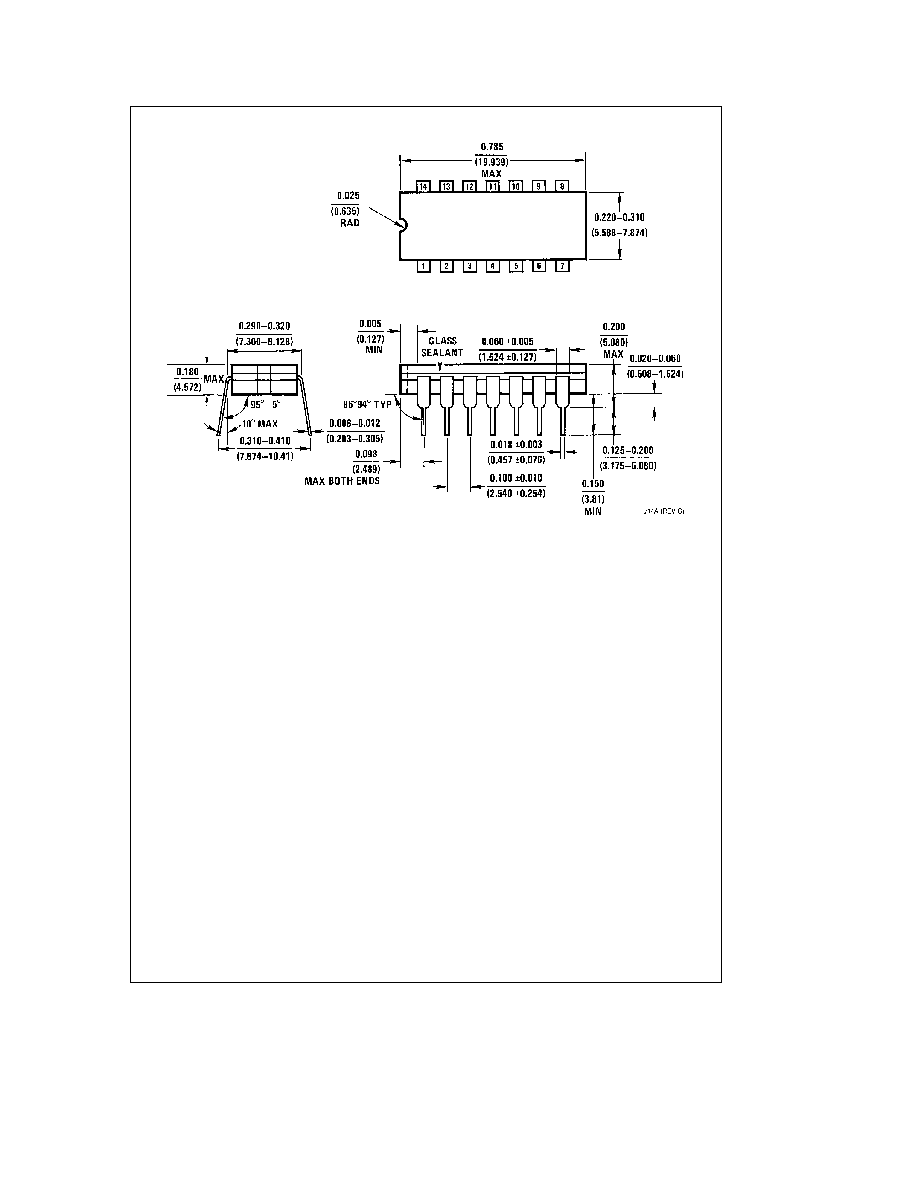
Physical Dimensions
inches (millimeters)
Ceramic Dual-In-Line Package (J)
Order Number CD4002MJ CD4002CJ CD4012MJ or CD4012CJ
NS Package Number J14A
5