 | –≠–ª–µ–∫—Ç—Ä–æ–Ω–Ω—ã–π –∫–æ–º–ø–æ–Ω–µ–Ω—Ç: CD4008BM | –°–∫–∞—á–∞—Ç—å:  PDF PDF  ZIP ZIP |
TL F 5944
CD4008BMCD4008BC
4-Bit
Full
Adder
February 1988
CD4008BM CD4008BC 4-Bit Full Adder
General Description
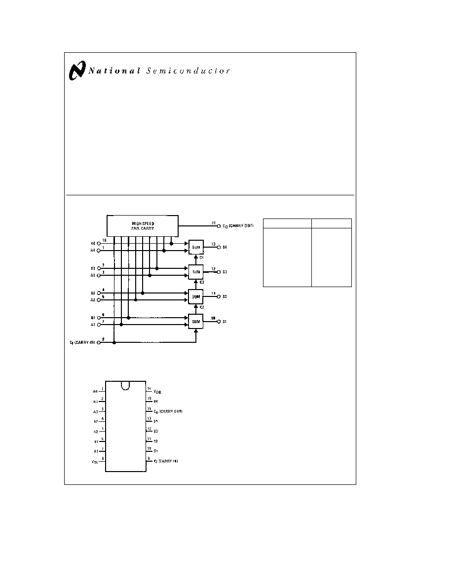
The CD4008B types consist of four full-adder stages with
fast look-ahead carry provision from stage to stage Circuitry
is included to provide a fast ``parallel-carry-out'' bit to permit
high-speed operation in arithmetic sections using several
CD4008B's CD4008B inputs include the four sets of bits to
be added A1 to A4 and B1 to B4 in addition to the ``Carry
in'' bit from a previous section CD4008B outputs include
the four sum bits S1 and S4 in addition to the high-speed
``parallel-carry-out'' which may be utilized at a succeeding
CD4008B section
All inputs are protected from damage due to static dis-
charge by diode clamps to V
DD
and GND
Features
Y
Wide supply voltage range
3 0V to 15V
Y
High noise immunity
0 45 V
CC
(typ )
Y
Low power TTL
Fan out of 2 driving 74L
compatibility
or 1 driving 74LS
Y
4 sum outputs plus parallel look-ahead carry-output
Y
Quiescent current specified to 15V
Y
Maximum input leakage of 1 mA at 15V (full package
temperature range)
Block Diagram
TL F 5944 ≠ 1
Truth Table
A
i
B
i
C
i
C0
SUM
0
0
0
0
0
1
0
0
0
1
0
1
0
0
1
1
1
0
1
0
0
0
1
0
1
1
0
1
1
0
0
1
1
1
0
1
1
1
1
1
Connection Diagram
Dual-In-Line Package
TL F 5944 ≠ 2
Top View
Order Number CD4008B
C1995 National Semiconductor Corporation
RRD-B30M105 Printed in U S A
Absolute Maximum Ratings
(Notes 1
2)
If Military Aerospace specified devices are required
please contact the National Semiconductor Sales
Office Distributors for availability and specifications
DC Supply Voltage (V
DD
)
b
0 5V to
a
18 V
DC
Input Voltage (V
IN
)
b
0 5V to V
DD
a
0 5 V
DC
Storage Temperature Range (T
S
)
b
65 C to
a
150 C
Power Dissipation (P
D
)
Dual-In-Line
700 mW
Small Outline
500 mW
Lead Temperature (T
L
)
(Soldering 10 seconds)
260 C
Recommended Operating
Conditions
(Note 2)
DC Supply Voltage (V
DD
)
3 to 15 V
DC
Input Voltage (V
IN
)
0 to V
DD
V
DC
Operating Temperature Range (T
A
)
CD4008BM
b
55 C to
a
125 C
CD4008BC
b
40 C to
a
85 C
DC Electrical Characteristics
CD4008BM (Note 2)
Symbol
Parameter
Conditions
b
55 C
a
25 C
a
125 C
Units
Min
Max
Min
Typ
Max
Min
Max
I
DD
Quiescent Device Current
V
DD
e
5V V
IN
e
V
DD
or V
SS
5
0 3
5
150
m
A
V
DD
e
10V V
IN
e
V
DD
or V
SS
10
0 5
10
300
m
A
V
DD
e
15V V
IN
e
V
DD
or V
SS
20
1 0
20
600
m
A
V
OL
Low Level Output Voltage
l
I
O
l
k
1mA
V
DD
e
5V
0 05
0
0 05
0 05
V
V
DD
e
10V
0 05
0
0 05
0 05
V
V
DD
e
15V
0 05
0
0 05
0 05
V
V
OH
High Level Output Voltage
l
I
O
l
k
1 mA
V
DD
e
5V
4 95
4 95
5
4 95
V
V
DD
e
10V
9 95
9 95
10
9 95
V
V
DD
e
15V
14 95
14 95
15
14 95
V
V
IL
Low Level Input Voltage
l
I
O
l
k
1 mA
V
DD
e
5V V
O
e
0 5V or 4 5V
1 5
1 5
1 5
V
V
DD
e
10V V
O
e
1V or 9V
3 0
3 0
3 0
V
V
DD
e
15V V
O
e
1 5V or 13 5V
4 0
4 0
4 0
V
V
IH
High Level Input Voltage
l
I
O
l
k
1 mA
V
DD
e
5V V
O
e
0 5V or 4 5V
3 5
3 5
3 5
V
V
DD
e
10V V
O
e
1V or 9V
7 0
7 0
7 0
V
V
DD
e
15V V
O
e
1 5V or 13 5V
11 0
11 0
11 0
V
I
OL
Low Level Output Current
V
DD
e
5V V
O
e
0 4V
0 64
0 51
0 88
0 36
mA
(Note 3)
V
DD
e
10V V
O
e
0 5V
1 6
1 3
2 25
0 9
mA
V
DD
e
15V V
O
e
1 5V
4 2
3 4
8 8
2 4
mA
I
OH
High Level Output Current V
DD
e
5V V
O
e
4 6V
b
0 25
b
0 2
b
0 35
b
0 14
mA
(Note 3)
V
DD
e
10V V
O
e
9 5V
b
0 62
b
0 5
b
0 8
b
0 35
mA
V
DD
e
15V V
O
e
13 5V
b
1 8
b
1 5
b
3 5
b
1 1
mA
I
IN
Input Current
V
DD
e
15V V
IN
e
0V
b
0 1
b
10
b
5
b
0 1
b
1 0
m
A
V
DD
e
15V V
IN
e
15V
0 1
10
b
5
0 1
1 0
m
A
DC Electrical Characteristics
CD4008BC (Note 2)
Symbol
Parameter
Conditions
b
40 C
a
25 C
a
85 C
Units
Min
Max
Min
Typ
Max
Min
Max
I
DD
Quiescent Device Current
V
DD
e
5V V
IN
e
V
DD
or V
SS
20
0 5
20
150
m
A
V
DD
e
10V V
IN
e
V
DD
or V
SS
40
1
40
300
m
A
V
DD
e
15V V
IN
e
V
DD
or V
SS
80
5
80
600
m
A
V
OL
Low Level Output Voltage
l
I
O
l
k
1 mA
V
DD
e
5V
0 05
0
0 05
0 05
V
V
DD
e
10V
0 05
0
0 05
0 05
V
V
DD
e
15V
0 05
0
0 05
0 05
V
V
OH
High Level Output Voltage
l
I
O
l
k
1 mA
V
DD
e
5V
4 95
4 95
5
4 95
V
V
DD
e
10V
9 95
9 95
10
9 95
V
V
DD
e
15V
14 95
14 95
15
14 95
V
2
DC Electrical Characteristics
CD4008BC (Note 2) (Continued)
Symbol
Parameter
Conditions
b
40 C
a
25 C
a
85 C
Units
Min
Max
Min
Typ
Max
Min
Max
V
IL
Low Level Input Voltage
l
I
O
l
k
1 mA
V
DD
e
5V V
O
e
0 5V or 4 5V
1 5
1 5
1 5
V
V
DD
e
10V V
O
e
1V or 9V
3 0
3 0
3 0
V
V
DD
e
15V V
O
e
1 5V or 13 5V
4 0
4 0
4 0
V
V
IH
High Level Input Voltage
l
I
O
l
k
1 mA
V
DD
e
5V V
O
e
0 5V or 4 5V
3 5
3 5
3 5
V
V
DD
e
10V V
O
e
1V or 9V
7 0
7 0
7 0
V
V
DD
e
15V V
O
e
1 5V or 13 5V
11 0
11 0
11 0
V
I
OL
Low Level Output Current
V
DD
e
5V V
O
e
0 4V
0 52
0 44
0 88
0 36
mA
(Note 3)
V
DD
e
10V V
O
e
0 5V
1 3
1 1
2 25
0 9
mA
V
DD
e
15V V
O
e
1 5V
3 6
3 0
8 8
2 4
mA
I
OH
High Level Output Current V
DD
e
5V V
O
e
4 6V
b
0 2
b
0 16
b
0 35
b
0 12
mA
(Note 3)
V
DD
e
10V V
O
e
9 5V
b
0 5
b
0 4
b
0 8
b
0 3
mA
V
DD
e
15V V
O
e
13 5V
b
1 4
b
1 2
b
3 5
b
1 0
mA
I
IN
Input Current
V
DD
e
15V V
IN
e
0V
b
0 3
b
0 3
b
1 0
m
A
V
DD
e
15V V
IN
e
15V
0 3
0 3
1 0
m
A
AC Electrical Characteristics
T
A
e
25 C C
L
e
50 pF R
L
e
200k input t
r
t
f
e
20 ns unless otherwise specified
Symbol
Parameter
Conditions
Min
Typ
Max
Units
t
PHL
or t
PLH
Propagation Delay Time
V
DD
e
5V
425
750
ns
Sum In to Sum Out
V
DD
e
10V
170
250
ns
V
DD
e
15V
125
190
ns
Carry In to Sum Out
V
DD
e
5V
320
650
ns
V
DD
e
10V
125
225
ns
V
DD
e
15V
95
175
ns
Sum In to Carry Out
V
DD
e
5V
250
500
ns
V
DD
e
10V
115
200
ns
V
DD
e
15V
90
160
ns
Carry In to Carry Out
V
DD
e
5V
130
245
ns
V
DD
e
10V
60
105
ns
V
DD
e
15V
45
80
ns
Carry In to Carry Out
C
L
e
15 pF
V
DD
e
5V
100
175
ns
V
DD
e
10V
45
75
ns
V
DD
e
15V
35
60
ns
t
THL
High-to-Low Transition Time
V
DD
e
5V
100
200
ns
V
DD
e
10V
50
100
ns
V
DD
e
15V
40
80
ns
t
TLH
Low-to-High Transition Time
V
DD
e
5V
200
400
ns
V
DD
e
10V
100
200
ns
V
DD
e
15V
80
160
ns
C
IN
Average Input Capacitance
5
7 5
pF
C
PD
Power Dissipation Capacitance
(Note 4)
100
pF
AC Parameters are guaranteed by DC correlated testing
Note 1
``Absolute Maximum Ratings'' are those values beyond which the safety of the device cannot be guaranteed they are not meant to imply that the devices
should be operated at these limits The table of ``Recommended Operating Conditions'' and ``Electrical Characteristics'' provides conditions for actual device
operation
Note 2
V
SS
e
0V unless otherwise specified
Note 3
I
OH
and I
OL
are tested one output at a time
Note 4
C
PD
determines the no load AC power consumption of any CMOS device For complete explanation see 54C 74C Family Characteristics application note
AN-90
3
AC Test Circuit and Switching Time Waveforms
C
L
e
50 pF
TL F 5944 ≠ 3
TL F 5944 ≠ 4
4
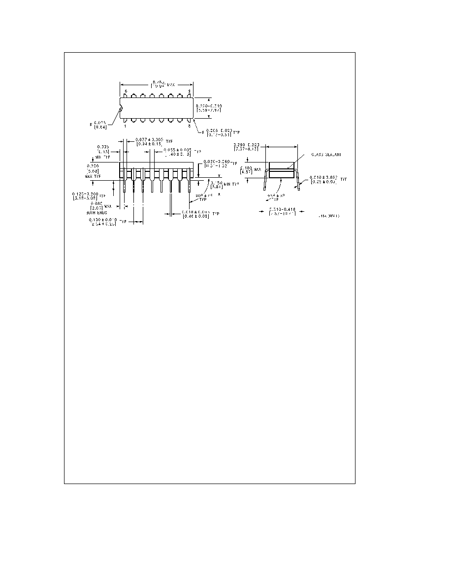
Physical Dimensions
inches (millimeters)
Ceramic Dual-In-Line Package (J)
Order Number CD4008BMJ or CD4008BCJ
NS Package Number J16A
5