Äîêóìåíòàöèÿ è îïèñàíèÿ www.docs.chipfind.ru
TL F 5987
CD40174BMCD40174BC
Hex
D
Flip-Flop
CD40175BMCD40175BC
Quad
D
Flip-Flop
February 1988
CD40174BM CD40174BC Hex D Flip-Flop
CD40175BM CD40175BC Quad D Flip-Flop
General Description
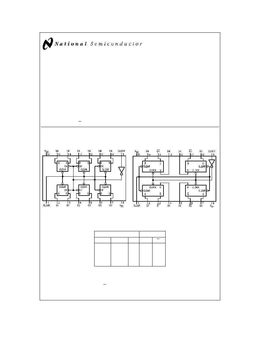
The CD40174B consists of six positive-edge triggered
D-type flip-flops the true outputs from each flip-flop are ex-
ternally available The CD40175B consists of four positive-
edge triggered D-type flip-flops both the true and comple-
ment outputs from each flip-flop are externally available
All flip-flops are controlled by a common clock and a com-
mon clear Information at the D inputs meeting the set-up
time requirements is transferred to the Q outputs on the
positive-going edge of the clock pulse The clearing opera-
tion enabled by a negative pulse at Clear input clears all Q
outputs to logical ``0'' and Qs (CD40175B only) to logical ``1''
All inputs are protected from static discharge by diode
clamps to V
DD
and V
SS
Features
Y
Wide supply voltage range
3V to 15V
Y
High noise immunity
0 45 V
DD
(typ )
Y
Low power TTL
fan out of 2 driving 74L
compatibility
or 1 driving 74 LS
Y
Equivalent to MC14174B MC14175B
Y
Equivalent to MM74C174 MM74C175
Connection Diagrams
CD40174B
Dual-In-Line Package
TL F 5987 1
Top View
Order Number CD40174B or CD40175B
Truth Table
Inputs
Outputs
Clear
Clock
D
Q
Q
L
X
X
L
H
H
u
H
H
L
H
u
L
L
H
H
H
X
NC
NC
H
L
X
NC
NC
H
e
High level
L
e
Low level
X
e
Irrelevant
u
e
Transition from low to high level
NC
e
No change
e
Q for CD40175B only
CD40175B
Dual-In-Line Package
TL F 5987 2
Top View
C1995 National Semiconductor Corporation
RRD-B30M105 Printed in U S A
Absolute Maximum Ratings
(Notes 1
2)
If Military Aerospace specified devices are required
please contact the National Semiconductor Sales
Office Distributors for availability and specifications
DC Supply Voltage (V
DD
)
b
0 5V to
a
18V
Input Voltage (V
IN
)
b
0 5V to V
DD
a
0 5V
DC
Storage Temperature Range (T
S
)
b
65 C to
a
150 C
Power Dissipation (P
D
)
Dual-In-Line
700 mW
Small Outline
500 mW
Lead Temperature (T
L
)
(Soldering 10 seconds)
260 C
Recommended Operating
Conditions
(Note 2)
DC Supply Voltage (V
DD
)
3V to 15 V
DC
Input Voltage (V
IN
)
0V to V
DD
V
DC
Operating Temperature Range (T
A
)
CD40XXXBM
b
55 C to
a
125 C
CD40XXXBC
b
40 C to
a
85 C
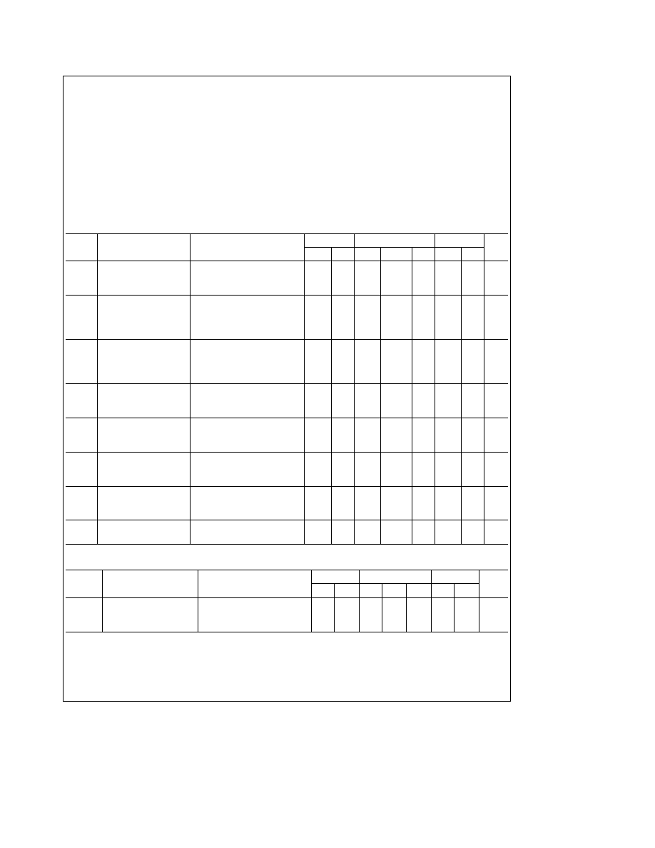
DC Electrical Characteristics
CD40174BM CD40175BM (Note 2)
Symbol
Parameter
Conditions
b
55 C
a
25 C
a
125 C
Units
Min
Max
Min
Typ
Max
Min
Max
I
DD
Quiescent Device Current
V
DD
e
5V V
IN
e
V
DD
or V
SS
1 0
1 0
30
m
A
V
DD
e
10V V
IN
e
V
DD
or V
SS
2 0
2 0
60
m
A
V
DD
e
15V V
IN
e
V
DD
or V
SS
4 0
4 0
120
m
A
V
OL
Low Level Output Voltage
l
I
O
l
k
1 mA
V
DD
e
5V
0 05
0 05
0 05
V
V
DD
e
10V
0 05
0 05
0 05
V
V
DD
e
15V
0 05
0 05
0 05
V
V
OH
High Level Output Voltage
l
I
O
l
k
1 mA
V
DD
e
5V
4 95
4 95
5
4 95
V
V
DD
e
10V
9 95
9 95
10
9 95
V
V
DD
e
15V
14 95
14 95
15
14 95
V
V
IL
Low Level Input Voltage
V
DD
e
5V V
O
e
0 5V or 4 5V
1 5
1 5
1 5
V
V
DD
e
10V V
O
e
1V or 9V
3 0
3 0
3 0
V
V
DD
e
15V V
O
e
1 5V or 13 5V
4 0
4 0
4 0
V
V
IH
High Level Input Voltage
V
DD
e
5V V
O
e
0 5V or 4 5V
3 5
3 5
3 5
V
V
DD
e
10V V
O
e
1V or 9V
7 0
7 0
7 0
V
V
DD
e
15V V
O
e
1 5V or 13 5V
11 0
11 0
11 0
V
I
OL
Low Level Output Current
V
DD
e
5V V
O
e
0 4V
0 64
0 51
0 88
0 36
mA
(Note 3)
V
DD
e
10V V
O
e
0 5V
1 6
1 3
2 25
0 9
mA
V
DD
e
15V V
O
e
1 5V
4 2
3 4
8 8
2 4
mA
I
OH
High Level Output Current
V
DD
e
5V V
O
e
4 6V
b
0 64
b
0 51
b
0 8 8
b
0 36
mA
(Note 3)
V
DD
e
10V V
O
e
9 5V
b
1 6
b
1 3
b
2 25
b
0 9
mA
V
DD
e
15V V
O
e
13 5V
b
4 2
b
3 4
b
8 8
b
2 4
mA
I
IN
Input Current
V
DD
e
15V V
IN
e
0V
b
0 1
b
10
b
5
b
0 1
b
1 0
m
A
V
DD
e
15V V
IN
e
15V
0 1
10
b
5
0 1
1 0
m
A
DC Electrical Characteristics
CD40174BC CD40175BC (Note 2)
Symbol
Parameter
Conditions
b
40 C
a
25 C
a
85 C
Units
Min
Max
Min
Typ
Max
Min
Max
I
DD
Quiescent Device Current
V
DD
e
5V V
IN
e
V
DD
or V
SS
4
4
30
m
A
V
DD
e
10V V
IN
e
V
DD
or V
SS
8
8
60
m
A
V
DD
e
15V V
IN
e
V
DD
or V
SS
16
16
120
m
A
Note 1
``Absolute Maximum Ratings'' are those values beyond which the safety of the device cannot be guaranteed They are not meant to imply that the devices
should be operated at these limits The tables of ``Recommended Operating Conditions'' and ``Electrical Characteristics'' provide conditions for actual device
operation
Note 2
V
SS
e
0V unless otherwise specified
Note 3
I
OH
and I
OL
are tested one output at a time
2

DC Electrical Characteristics
CD40174BC CD40175BC (Note 2) (Continued)
Symbol
Parameter
Conditions
b
40 C
a
25 C
a
85 C
Units
Min
Max
Min
Typ
Max
Min
Max
V
OL
Low Level Output Voltage V
DD
e
5V
0 05
0 05
0 05
V
V
DD
e
10V
0 05
0 05
0 05
V
V
DD
e
15V
0 05
0 05
0 05
V
V
OH
High Level Output Voltage V
DD
e
5V
4 95
4 95
5
4 95
V
V
DD
e
10V
9 95
9 95
10
9 95
V
V
DD
e
15V
14 95
14 95
15
14 95
V
V
IL
Low Level Input Voltage
V
DD
e
5V V
O
e
0 5V or 4 5V
1 5
1 5
1 5
V
V
DD
e
10V V
O
e
1V or 9V
3 0
3 0
3 0
V
V
DD
e
15V V
O
e
1 5V or 13 5V
4 0
4 0
4 0
V
V
IH
High Level Input Voltage
V
DD
e
5V V
O
e
0 5V or 4 5V
3 5
3 5
3 5
V
V
DD
e
10V V
O
e
1V or 9V
7 0
7 0
7 0
V
V
DD
e
15V V
O
e
1 5V or 13 5V
11 0
11 0
11 0
V
I
OL
Low Level Output Current V
DD
e
5V V
O
e
0 4V
0 52
0 44
0 88
0 36
mA
(Note 3)
V
DD
e
10V V
O
e
0 5V
1 3
1 1
2 25
0 9
mA
V
DD
e
15V V
O
e
1 5V
3 6
3 0
8 8
2 4
mA
I
OH
High Level Output Current V
DD
e
5V V
O
e
4 6V
b
0 52
b
0 44
b
0 88
b
0 36
mA
(Note 3)
V
DD
e
10V V
O
e
9 5V
b
1 3
b
1 1
b
2 25
b
0 9
mA
V
DD
e
15V V
O
e
13 5V
b
3 6
b
3 0
b
8 8
b
2 4
mA
I
IN
Input Current
V
DD
e
15V V
IN
e
0V
b
0 30
b
10
b
5
b
0 30
b
1 0
m
A
V
DD
e
15V V
IN
e
15V
0 30
10
b
5
0 30
1 0
m
A
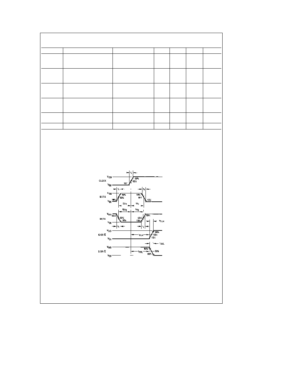
AC Electrical Characteristics
T
A
e
25 C C
L
e
50 pF R
L
e
200k and t
r
e
t
f
e
20 ns unless otherwise specified
Symbol
Parameter
Conditions
Min
Typ
Max
Units
t
PHL
t
PLH
Propagation Delay Time to a
V
DD
e
5V
190
300
ns
Logical ``0'' or Logical ``1'' from
V
DD
e
10V
75
110
ns
Clock to Q or Q (CD40175 Only)
V
DD
e
15V
60
90
ns
t
PHL
Propagation Delay Time to a
V
DD
e
5V
180
300
ns
Logical ``0'' from Clear to Q
V
DD
e
10V
70
110
ns
V
DD
e
15V
60
90
ns
t
PLH
Propagation Delay Time to a Logical
V
DD
e
5V
230
400
ns
``1'' from Clear to Q (CD40175 Only)
V
DD
e
10V
90
150
ns
V
DD
e
15V
75
120
ns
t
SU
Time Prior to Clock Pulse that
V
DD
e
5V
45
100
ns
Data must be Present
V
DD
e
10V
15
40
ns
V
DD
e
15V
13
35
ns
t
H
Time after Clock Pulse that
V
DD
e
5V
b
11
0
ns
Data Must be Held
V
DD
e
10V
b
4
0
ns
V
DD
e
15V
b
3
0
ns
t
THL
t
TLH
Transition Time
V
DD
e
5V
100
200
ns
V
DD
e
10V
50
100
ns
V
DD
e
15V
40
80
ns
t
WH
t
WL
Minimum Clock Pulse Width
V
DD
e
5V
130
250
ns
V
DD
e
10V
45
100
ns
V
DD
e
15V
40
80
ns
3
AC Electrical Characteristics
T
A
e
25 C C
L
e
50 pF R
L
e
200k and t
r
e
t
f
e
20 ns unless otherwise specified (Continued)
Symbol
Parameter
Conditions
Min
Typ
Max
Units
t
WL
Minimum Clear Pulse Width
V
DD
e
5V
120
250
ns
V
DD
e
10V
45
100
ns
V
DD
e
15V
40
80
ns
t
RCL
Maximum Clock Rise Time
V
DD
e
5V
15
m
s
V
DD
e
10V
5 0
m
s
V
DD
e
15V
5 0
m
s
t
fCL
Maximum Clock Fall Time
V
DD
e
5V
15
50
m
s
V
DD
e
10V
5 0
50
m
s
V
DD
e
15V
5 0
50
m
s
f
CL
Maximum Clock Frequency
V
DD
e
5V
2 0
3 5
MHz
V
DD
e
10V
5 0
10
MHz
V
DD
e
15V
6 0
12
MHz
C
IN
Input Capacitance
Clear Input
10
15
pF
Other Input
5 0
7 5
pF
C
PD
Power Dissipation
Per Package (Note 4)
130
pF
AC Parameters are guaranteed by DC correlated testing
Note 1
``Absolute Maximum Ratings'' are those values beyond which the safety of the device cannot be guaranteed They are not meant to imply that the
devices should be operated at these limits The tables of ``Recommended Operating Conditions'' and ``Electrical Characteristics'' provide conditions for actual
device operation
Note 2
V
SS
e
0V unless otherwise specified
Note 3
I
OH
and I
OL
are tested one output at a time
Note 4
C
PD
determines the no load AC power consumption of any CMOS device For complete explanation see 54C 74C Family Characteristics application
note AN-90
Switching Time Waveforms
TL F 5987 3
t
r
e
t
f
e
20 ns
4

Physical Dimensions
inches (millimeters)
Ceramic Dual-In-Line Package (J)
Order Number CD40174BMJ CD40174BCJ CD40175BMJ or CD40175BCJ
NS Package Number J16A
5