TL F 5956
CD4023BMCD4023BC
Buffered
Triple
3-Input
NAND
Gate
CD4025BMCD4025BC
Buffered
Triple
3-Input
NOR
Gate
February 1988
CD4023BM CD4023BC
Buffered Triple 3-Input NAND Gate
CD4025BM CD4025BC
Buffered Triple 3-Input NOR Gate
General Description
These triple gates are monolithic complementary MOS
(CMOS) integrated circuits constructed with N- and P-chan-
nel enhancement mode transistors They have equal source
and sink current capabilities and conform to standard B se-
ries output drive The devices also have buffered outputs
which improve transfer characteristics by providing very
high gain All inputs are protected against static discharge
with diodes to V
DD
and V
SS
Features
Y
Wide supply voltage range
3 0V to 15V
Y
High noise immunity
0 45 V
DD
(typ )
Y
Low power TTL
fan out of 2 driving 74L
compatibility
or 1 driving 74LS
Y
5V � 10V � 15V parametric ratings
Y
Symmetrical output characteristics
Y
Maximum input leakage 1 mA at 15V over full
temperature range
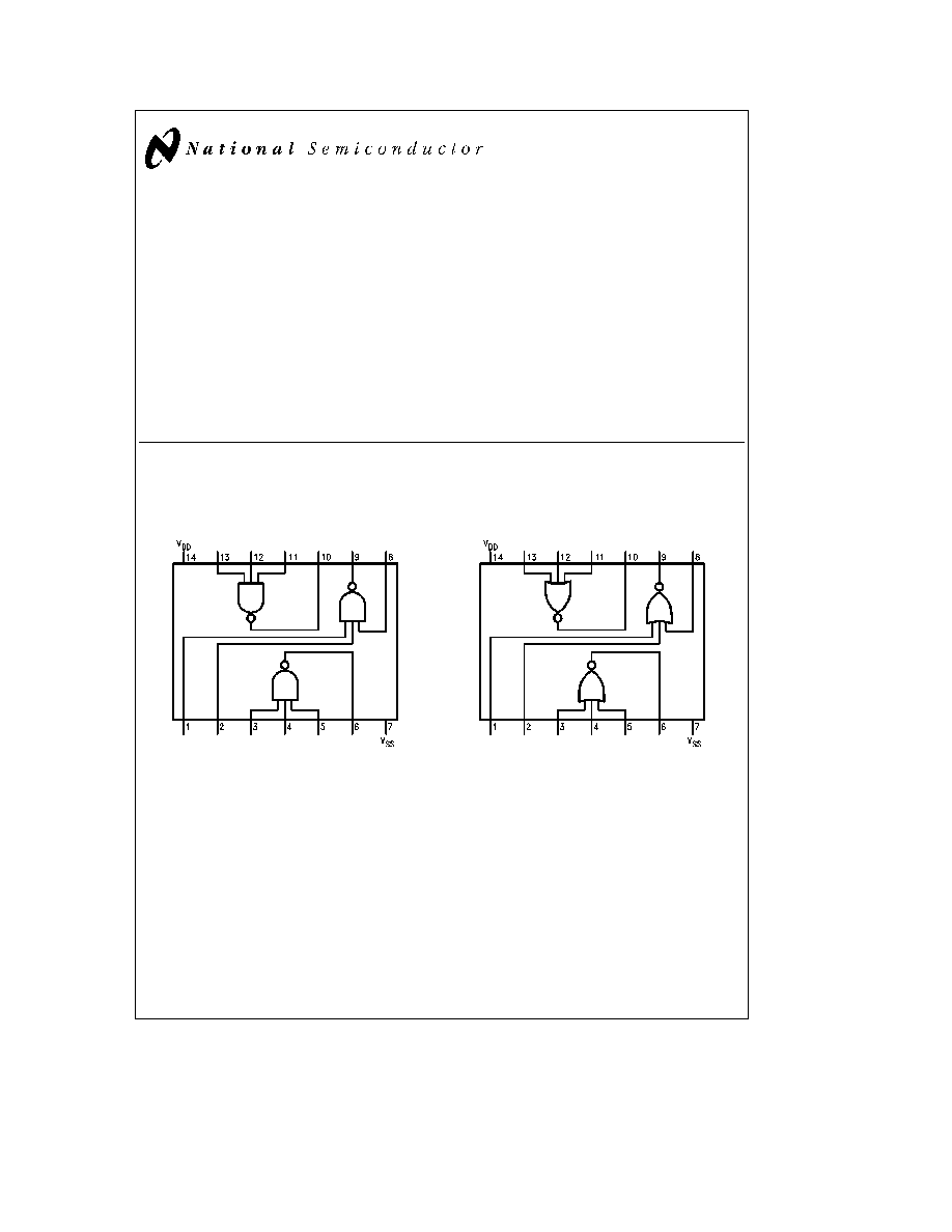
Connection Diagrams
CD4023BM CD4023BC
Dual-In-Line Package
TL F 5956 � 1
Top View
CD4025BM CD4025BC
Dual-In-Line Package
TL F 5956 � 2
Top View
Order Number CD4023B or CD4025B
C1995 National Semiconductor Corporation
RRD-B30M105 Printed in U S A
Absolute Maximum Ratings
(Notes 1
2)
If Military Aerospace specified devices are required
please contact the National Semiconductor Sales
Office Distributors for availability and specifications
DC Supply Voltage (V
DD
)
b
0 5 V
DC
to
a
18 V
DC
Input Voltage (V
IN
)
b
0 5 V
DC
to V
DD
a
0 5 V
DC
Storage Temp Range (T
S
)
b
65 C to
a
150 C
Power Dissipation (P
D
)
Dual-In-Line
700 mW
Small Outline
500 mW
Lead Temperature (T
L
)
(Soldering 10 seconds)
260 C
Recommended Operating
Conditions
DC Supply Voltage (V
DD
)
5 V
DC
to 15 V
DC
Input Voltage (V
IN
)
0 V
DC
to V
DD
V
DC
Operating Temperature Range (T
A
)
CD4023BM CD4025BM
b
55 C to
a
125 C
CD4023BC CD4025BC
b
40 C to
a
85 C
DC Electrical Characteristics
CD4023BM CD4025BM (Note 2)
Symbol
Parameter
Conditions
b
55 C
a
25 C
a
125 C
Units
Min
Typ
Min
Typ
Max
Min
Max
I
DD
Quiescent Device Current V
DD
e
5V
0 25
0 004
0 25
7 5
m
A
V
DD
e
10V
0 5
0 005
0 5
15
m
A
V
DD
e
15V
1 0
0 006
1 0
30
m
A
V
OL
Low Level Output Voltage V
DD
e
5V
0 05
0
0 05
0 05
V
V
DD
e
10V
0 05
0
0 05
0 05
V
V
DD
e
15V
0 05
0
0 05
0 05
V
V
OH
High Level Output Voltage V
DD
e
5V
4 95
4 95
5
4 95
V
V
DD
e
10V
9 95
9 95
10
9 95
V
V
DD
e
15V
14 95
14 95
15
14 95
V
V
IL
Low Level Input Voltage
V
DD
e
5V V
O
e
4 5V
1 5
2
1 5
1 5
V
V
DD
e
10V V
O
e
9 0V
l
I
O
l
k
1mA
3 0
4
3 0
3 0
V
V
DD
e
15V V
O
e
13 5V
(
4 0
6
4 0
4 0
V
V
IH
High Level Input Voltage
V
DD
e
5V V
O
e
0 5V
3 5
3 5
3
3 5
V
V
DD
e
10V V
O
e
1 0V
l
I
O
l
k
1mA
7 0
7 0
6
7 0
V
V
DD
e
15V V
O
e
1 5V
(
11 0
11 0
9
11 0
V
I
OL
Low Level Output Current V
DD
e
5V V
O
e
0 4V
0 64
0 51
0 88
0 36
mA
(Note 3)
V
DD
e
10V V
O
e
0 5V
1 6
1 3
2 2
0 90
mA
V
DD
e
15V V
O
e
1 5V
4 2
3 4
8
2 4
mA
I
OH
High Level Output Current V
DD
e
5V V
O
e
4 6V
b
0 64
b
0 51
b
0 88
b
0 36
mA
(Note 3)
V
DD
e
10V V
O
e
9 5V
b
1 6
b
1 3
b
2 2
b
0 90
mA
V
DD
e
15V V
O
e
13 5V
b
4 2
b
3 4
b
8
b
2 4
mA
I
IN
Input Current
V
DD
e
15V V
IN
e
0V
b
0 10
b
10
b
5
b
0 10
b
1 0
m
A
V
DD
e
15V V
IN
e
15V
0 10
10
b
5
0 10
1 0
m
A
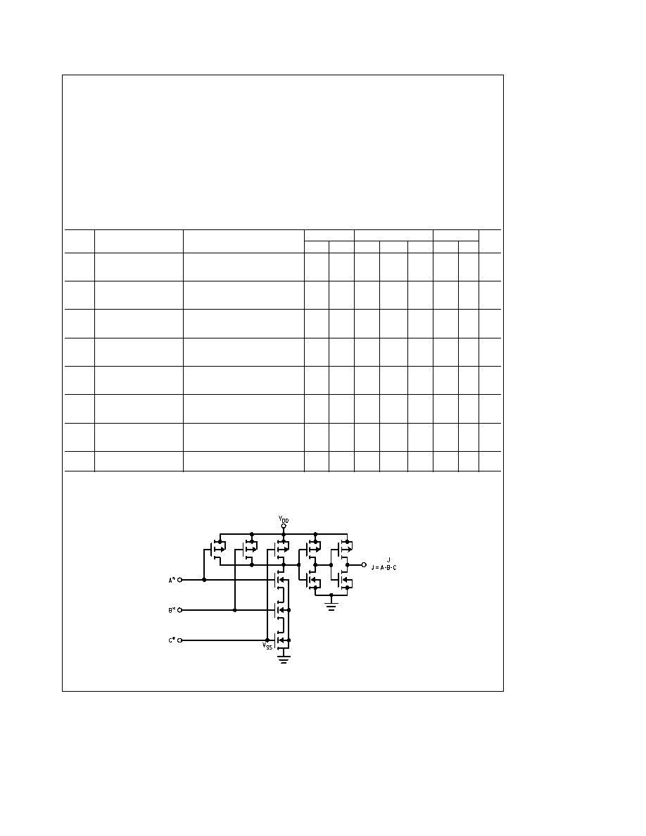
Schematic Diagram
CD4023BC CD4023BM
TL F 5956 � 3
Device Shown
All Inputs Protected
by Standard CMOS Input
Protection Circuit
2
DC Electrical Characteristics
CD4023BC CD4025BC (Note 2)
Symbol
Parameter
Conditions
b
40 C
a
25 C
a
85 C
Units
Min
Typ
Min
Typ
Max
Min
Max
I
DD
Quiescent Device Current V
DD
e
5V
1 0
0 004
1 0
7 5
m
A
V
DD
e
10V
2 0
0 005
2 0
15
m
A
V
DD
e
15V
4 0
0 006
4 0
30
m
A
V
OL
Low Level Output Voltage V
DD
e
5V
0 05
0
0 05
0 05
V
V
DD
e
10V
0 05
0
0 05
0 05
V
V
DD
e
15V
0 05
0
0 05
0 05
V
V
OH
High Level Output Voltage V
DD
e
5V
4 95
4 95
5
4 95
V
V
DD
e
10V
9 95
9 95
10
9 95
V
V
DD
e
15V
14 95
14 95
15
14 95
V
V
IL
Low Level Input Voltage
V
DD
e
5V V
O
e
4 5V
1 5
2
1 5
1 5
V
V
DD
e
10V V
O
e
9 0V
l
I
O
l
k
1mA
3 0
4
3 0
3 0
V
V
DD
e
15V V
O
e
13 5V
(
4 0
6
4 0
4 0
V
V
IH
High Level Input Voltage
V
DD
e
5V V
O
e
0 5V
3 5
3 5
3
3 5
V
V
DD
e
10V V
O
e
1 0V
l
I
O
l
k
1mA
7 0
7 0
6
7 0
V
V
DD
e
15V V
O
e
1 5V
(
11 0
11 0
9
11 0
V
I
OL
Low Level Output Current V
DD
e
5V V
O
e
0 4V
0 52
0 44
0 88
0 36
mA
(Note 3)
V
DD
e
10V V
O
e
0 5V
1 3
1 1
2 2
0 90
mA
V
DD
e
15V V
O
e
1 5V
3 6
3 0
8
2 4
mA
I
OH
High Level Output Current V
DD
e
5V V
O
e
4 6V
b
0 52
b
0 44
b
0 88
b
0 36
mA
(Note 3)
V
DD
e
10V V
O
e
9 5V
b
1 3
b
1 1
b
2 2
b
0 90
mA
V
DD
e
15V V
O
e
13 5V
b
3 6
b
3 0
b
8
b
2 4
mA
I
IN
Input Current
V
DD
e
15V V
IN
e
0V
b
0 3
b
10
b
5
b
0 3
b
1 0
m
A
V
DD
e
15V V
IN
e
15V
0 3
10
b
5
0 3
1 0
m
A
Note 1
``Absolute Maximum Ratings'' are those values beyond which the safety of the device cannot be guaranteed they are not meant to imply that the devices
should be operated at these limits The table of ``Recommended Operating Conditions'' and ``Electrical Characteristics'' provides conditions for actual device
operation
Note 2
V
SS
e
0V unless otherwise specified
Note 3
I
OH
and I
OL
are tested one output at a time
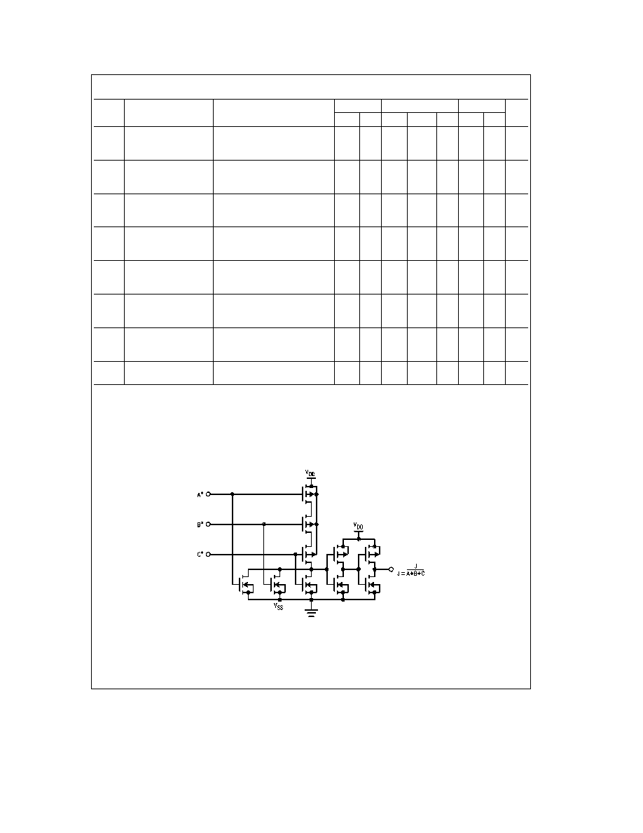
Schematic Diagram
CD4025BM CD4025BC
TL F 5956 � 4
Device Shown
All Inputs Protected
by Standard CMOS Input
Protection Circuit
3
AC Electrical Characteristics
T
A
e
25 C C
L
e
50 pF R
L
e
200k unless otherwise specified
CD4023BC
CD4025BC
Symbol
Parameter
Conditions
CD4023BM
CD4025BM
Units
Min
Typ
Max
Min
Typ
Max
t
PHL
Propagation Delay High-to-Low Level
V
DD
e
5V
130
250
130
250
ns
V
DD
e
10V
60
100
60
100
ns
V
DD
e
15V
40
70
40
70
ns
t
PLH
Propagation Delay Low-to-High Level
V
DD
e
5V
110
250
120
250
ns
V
DD
e
10V
50
100
60
100
ns
V
DD
e
15V
35
70
40
70
ns
t
THL
Transition Time
V
DD
e
5V
90
200
90
200
ns
t
TLH
V
DD
e
10V
50
100
50
100
ns
V
DD
e
15V
40
80
40
80
ns
C
IN
Average Input Capacitance
Any Input
5
7 5
5
7 5
pF
C
PD
Power Dissipation Capacity (Note 4)
Any Gate
17
17
pF
AC Parameters are guaranteed by DC correlated testing
Note 4
C
PD
determines the no load AC power consumption of any CMOS device For complete explanation see 54C 74C Family Characteristics Application
Note AN-90
4

Physical Dimensions
inches (millimeters)
Ceramic Dual-In-Line Package (J)
Order Number CD4023BMJ CD4023BCJ CD4025BMJ or CD4025BCJ
NS Package Number J14A
5