 | –≠–ª–µ–∫—Ç—Ä–æ–Ω–Ω—ã–π –∫–æ–º–ø–æ–Ω–µ–Ω—Ç: CD4035BM | –°–∫–∞—á–∞—Ç—å:  PDF PDF  ZIP ZIP |
TL F 5964
CD4035BMCD4035BC
4-Bit
Parallel-InParallel-Out
Shift
Register
February 1988
CD4035BM CD4035BC
4-Bit Parallel-In Parallel-Out Shift Register
General Description
The CD4035B 4-bit parallel-in parallel-out shift register is a
monolithic complementary MOS (CMOS) integrated circuit
constructed with P- and N-channel enhancement mode
transistors This shift register is a 4-stage clocked serial reg-
ister having provisions for synchronous parallel inputs to
each stage and serial inputs to the first stage via JK logic
Register stages 2 3 and 4 are coupled in a serial ``D'' flip-
flop configuration when the register is in the serial mode
(parallel serial control low)
Parallel entry via the ``D'' line of each register stage is per-
mitted only when the parallel serial control is ``high''
In the parallel or serial mode information is transferred on
positive clock transitions
When the true complement control is ``high'' the true con-
tents of the register are available at the output terminals
When the true complement control is ``low'' the outputs are
the complements of the data in the register The true com-
plement control functions asynchronously with respect to
the clock signal
JK input logic is provided on the first stage serial input to
minimize logic requirements particularly in counting and se-
quence-generation applications With JK inputs connected
together the first stage becomes a ``D'' flip-flop An asyn-
chronous common reset is also provided
Features
Y
Wide supply voltage range
3 0V to 15V
Y
High noise immunity
0 45 V
DD
(typ )
Y
Low power TTL
Fan out of 2 driving 74L
compatibility
or 1 driving 74LS
Y
4-stage clocked operation
Y
Synchronous parallel entry on all 4 stages
Y
JK inputs on first stage
Y
Asynchronous true complement control on all outputs
Y
Reset control
Y
Static flip-flop operation master slave configuration
Y
Buffered outputs
Y
Low power dissipation
5 mW (typ ) (ceramic)
Y
High speed
to 5 MHz
Applications
Y
Automotive
Y
Alarm systems
Y
Data terminals
Y
Industrial controls
Y
Instrumentation
Y
Remote metering
Y
Medical electronics
Y
Computers
Logic Diagram
TL F 5964 ≠ 1
P S
e
0
e
serial mode
T C
e
1
e
true outputs
TG
e
transmission gate
TL F 5964 ≠ 2
Input to output is
a) A bidirectional low impedance when control input 1 is low and control input 2 is high
b) An open circuit when control input 1 is high and control input 2 is low
C1995 National Semiconductor Corporation
RRD-B30M105 Printed in U S A
Absolute Maximum Ratings
(Notes 1 and 2)
If Military Aerospace specified devices are required
please contact the National Semiconductor Sales
Office Distributors for availability and specifications
DC Supply Voltage (V
DD
)
b
0 5V to
a
18V
Input Voltage (V
IN
)
b
0 5V to V
DD
a
0 5V
Storage Temperature Range (T
S
)
b
65 C to
a
150 C
Power Dissipation (P
D
)
Dual-In-Line
700 mW
Small Outline
500 mW
Lead Temperature (T
L
)
(Soldering 10 seconds)
260 C
Operating Conditions
(Note 2)
DC Supply Voltage (V
DD
)
3V to 15V
Input Voltage (V
IN
)
0V to V
DD
V
Operating Temperature Range (T
A
)
CD4035BM
b
55 C to
a
125 C
CD4035BC
b
40 C to
a
85 C
DC Electrical Characteristics
CD4035BM (Note 2)
Symbol
Parameter
Conditions
b
55 C
a
25 C
a
125 C
Units
Min
Max
Min
Typ
Max
Min
Max
I
DD
Quiescent Device Current V
DD
e
5V V
IN
e
V
DD
or V
SS
5
0 3
5
150
m
A
V
DD
e
10V V
IN
e
V
DD
or V
SS
10
0 5
10
300
m
A
V
DD
e
15V V
IN
e
V
DD
or V
SS
20
1 0
20
600
m
A
V
OL
Low Level Output Voltage
l
I
O
l
k
1 0 mA
V
DD
e
5V
0 05
0
0 05
0 05
V
V
DD
e
10V
0 05
0
0 05
0 05
V
V
DD
e
15V
0 05
0
0 05
0 05
V
V
OH
High Level Output Voltage
l
I
O
l
k
1 0 mA
V
DD
e
5V
4 95
4 95
5
4 95
V
V
DD
e
10V
9 95
9 95
10
9 95
V
V
DD
e
15V
14 95
14 95
15
14 95
V
V
IL
Low Level Input Voltage
l
I
O
l
k
1 0 mA
V
DD
e
5V
V
O
e
0 5V or 4 5V
1 5
1 5
1 5
V
V
DD
e
10V
V
O
e
1 0V or 9 0V
3 0
3 0
3 0
V
V
DD
e
15V
V
O
e
1 5V or 13 5V
4 0
4 0
4 0
V
V
IH
High Level Input Voltage
l
I
O
l
k
1 0 mA
V
DD
e
5V
V
O
e
0 5V or 4 5V
3 5
3 5
3 5
V
V
DD
e
10V
V
O
e
1 0V or 9 0V
7 0
7 0
7 0
V
V
DD
e
15V
V
O
e
1 5V or 13 5V
11 0
11 0
11 0
V
I
OL
Low Level Output Current
V
DD
e
5V
V
O
e
0 4V
0 64
0 51
0 88
0 36
mA
(Note 3)
V
DD
e
10V
V
O
e
0 5V
1 6
1 3
2 25
0 9
mA
V
DD
e
15V
V
O
e
1 5V
4 2
3 4
8 8
2 4
mA
I
OH
High Level Output Current V
DD
e
5V
V
O
e
4 6V
b
0 25
b
0 2
0 36
b
0 14
mA
(Note 3)
V
DD
e
10V
V
O
e
9 5V
b
0 62
b
0 5
0 9
b
0 35
mA
V
DD
e
15V
V
O
e
13 5V
b
1 8
b
1 5
b
3 5
b
1 1
mA
I
IN
Input Current
V
DD
e
15V
V
IN
e
0V
b
0 1
b
10
b
5
b
0 1
b
1 0
m
A
V
DD
e
15V
V
IN
e
15V
0 1
10
b
5
0 1
1 0
m
A
DC Electrical Characteristics
CD4035BC (Note 2)
Symbol
Parameter
Conditions
b
40 C
a
25 C
a
85 C
Units
Min
Max
Min
Typ
Max
Min
Max
I
DD
Quiescent Device Current
V
DD
e
5V V
IN
e
V
DD
or V
SS
20
0 5
20
150
m
A
V
DD
e
10V V
IN
e
V
DD
or V
SS
40
1 0
40
300
m
A
V
DD
e
15V V
IN
e
V
DD
or V
SS
80
5 0
80
600
m
A
V
OL
Low Level Output Voltage
l
I
O
l
k
1 mA
V
DD
e
5V
0 05
0
0 05
0 05
V
V
DD
e
10V
0 05
0
0 05
0 05
V
V
DD
e
15V
0 05
0
0 05
0 05
V
V
OH
High Level Output Voltage
l
I
O
l
k
1 mA
V
DD
e
5V
4 95
4 95
5
4 95
V
V
DD
e
10V
9 95
9 95
10
9 95
V
V
DD
e
15V
14 95
14 95
15
14 95
V
2
DC Electrical Characteristics
CD4035BC (Note 2) (Continued)
Symbol
Parameter
Conditions
b
40 C
25 C
85 C
Units
Min
Max
Min
Typ
Max
Min
Max
V
IL
Low Level Input Voltage
l
I
O
l
k
1 mA
V
DD
e
5V
V
O
e
0 5V or 4 5V
1 5
1 5
1 5
V
V
DD
e
10V
V
O
e
1 0V or 9 0V
3 0
3 0
3 0
V
V
DD
e
15V
V
O
e
1 5V or 13 5V
4 0
4 0
4 0
V
V
IH
High Level Input Voltage
l
I
O
l
k
1 mA
V
DD
e
5V
V
O
e
0 5V or 4 5V
3 5
3 5
3 5
V
V
DD
e
10V
V
O
e
1 0V or 9 0V
7 0
7 0
7 0
V
V
DD
e
15V
V
O
e
1 5V or 13 5V 11 0
11 0
11 0
V
I
OL
Low Level Output Current V
DD
e
5V
V
O
e
0 4V
0 52
0 44
0 88
0 36
mA
(Note 3)
V
DD
e
10V
V
O
e
0 5V
1 3
1 1
2 25
0 9
mA
V
DD
e
15V
V
O
e
1 5V
3 6
3 0
8 8
2 4
mA
I
OH
High Level Output Current V
DD
e
5V
V
O
e
4 6V
b
0 2
b
0 16
0 36
b
0 12
mA
(Note 3)
V
DD
e
10V
V
O
e
9 5V
b
0 5
b
0 4
0 9
b
0 3
mA
V
DD
e
15V
V
O
e
13 5V
b
1 4
b
1 2
b
3 5
b
1 0
mA
I
IN
Input Current
V
DD
e
15V
V
IN
e
0V
b
0 3
b
10
b
5
b
0 3
b
1 0
m
A
V
DD
e
15V
V
IN
e
15V
0 3
10
b
5
0 3
1 0
m
A
Note 1
``Absolute Maximum Ratings'' are those values beyond which the safety of the device cannot be guaranteed they are not meant to imply that the devices
should be operated at these limits The table of ``Recommended Operating Conditions'' and ``Electrical Characteristics'' provides conditions for actual device
operation
Note 2
V
SS
e
0V unless otherwise specified
Note 3
I
OH
and I
OL
are tested one output at a time
AC Electrical Characteristics
T
A
e
25 C C
L
e
50 pF R
L
e
200k t
r
and t
f
e
20 ns unless otherwise specified
Symbol
Parameter
Conditions
Min
Typ
Max
Units
CLOCKED OPERATION
t
PHL
t
PLH
Propagation Delay Time
V
DD
e
5V
250
500
ns
V
DD
e
10V
100
200
ns
V
DD
e
15V
75
150
ns
t
THL
Transition Time High
V
DD
e
5V
90
175
ns
Low to High
V
DD
e
10V
50
75
ns
V
DD
e
15V
40
60
ns
t
TLH
Transition Time
V
DD
e
5V
135
270
ns
Low to High
V
DD
e
10V
70
140
ns
V
DD
e
15V
60
120
ns
t
WL
t
WH
Minimum Clock Pulse Width
V
DD
e
5V
335
135
ns
V
DD
e
10V
165
50
ns
V
DD
e
15V
100
40
ns
t
rCL
t
fCL
Clock Rise and Fall Time
V
DD
e
5V
15
m
s
V
DD
e
10V
10
m
s
V
DD
e
15V
5
m
s
t
S
Minimum Set-up Time
J K Lines
V
DD
e
5V
250
500
ns
V
DD
e
10V
100
200
ns
V
DD
e
15V
80
160
ns
t
S
Parallel-In Lines
V
DD
e
5V
250
500
ns
V
DD
e
10V
100
200
ns
V
DD
e
15V
80
160
ns
t
S
P S Control
V
DD
e
5V
100
200
ns
V
DD
e
10V
40
80
ns
V
DD
e
15V
35
60
ns
f
MAX
Maximum Clock Frequency
V
DD
e
5V
1 5
2 5
MHz
V
DD
e
10V
3
6
MHz
V
DD
e
15V
5
9
MHz
3
AC Electrical Characteristics
T
A
e
25 C C
L
e
50 pF R
L
e
200k t
r
and t
f
e
20 ns unless otherwise specified (Continued)
Symbol
Parameter
Conditions
Min
Typ
Max
Units
CLOCKED OPERATION
(Continued)
C
IN
Input Capacitance
Any Input
5
7 5
pF
RESET OPERATION
t
PHL
t
PLH
Propagation Delay Time
V
DD
e
5V
300
500
ns
V
DD
e
10V
150
200
ns
V
DD
e
15V
85
150
ns
t
WH
Minimum Reset Pulse Width
V
DD
e
5V
75
250
ns
V
DD
e
10V
30
110
ns
V
DD
e
15V
25
80
ns
AC Parameters are guaranteed by DC correlated testing
Truth Table
C
L
t
n
b
1 (Inputs)
t
n
(Outputs)
J
K
R
Q
nb1
Q
n
L
0
X
0
0
0
L
I
X
0
0
I
L
X
0
0
I
0
L
I
0
0
Q
nb1
Q
nb1
TOGGLE
MODE
L
X
I
0
I
I
K
X
X
0
Q
nb1
Q
nb1
X
X
X
I
X
0
Switching Time Waveforms
TL F 5964 ≠ 3
T C Input Low
Reset Input Low
4
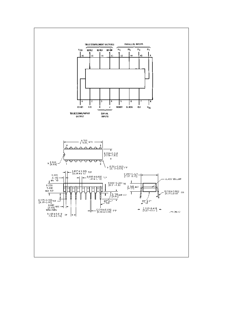
Connection Diagram
Dual-In-Line Package
TL F 5964 ≠ 4
Top View
Order Number CD4035B
Physical Dimensions
inches (millimeters)
Ceramic Dual-In-Line Package (J)
Order Number CD4035BMJ or CD4035BCJ
NS Package Number J16A
5