TL F 5976
CD4070BMCD4070BCCD4077BMCD4077BC
March 1992
CD4070BM CD4070BC
Quad 2-Input EXCLUSIVE-OR Gate
CD4077BM CD4077BC
Quad 2-Input EXCLUSIVE-NOR Gate
General Description
Employing complementary MOS (CMOS) transistors to
achieve wide power supply operating range low power con-
sumption and high noise margin the CD4070BM BC and
CD4077BM BC provide basic functions used in the imple-
mentation of digital integrated circuit systems The N- and
P-channel enhancement mode transistors provide a sym-
metrical circuit with output swing essentially equal to the
supply voltage No DC power other than that caused by
leakage current is consumed during static condition All in-
puts are protected from damage due to static discharge by
diode clamps to V
DD
and V
SS
Features
Y
Wide supply voltage range
3 0V to 15V
Y
High noise immunity
0 45 V
DD
typ
Y
Low power TTL
Fan out of 2 driving 74L
compatibility
or 1 driving 74LS
Y
CD4070B
Pin compatible to CD4030A
Equivalent to MM54C86 MM74C86
and MC14070B
Y
CD4077B
Equivalent to MC14077B
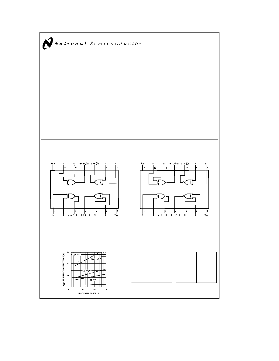
Connection Diagram
CD4070BM CD4070BC
Dual-In-Line Package
TL F 5976 � 1
Top View
CD4077BM CD4077BC
Dual-In-Line Package
TL F 5976 � 5
Top View
Typical Performance
Characteristics
Truth Tables
Propagation Delay Time
vs Load Capacitance
TL F 5976 � 2
CD4070BM CD4070BC
Inputs
Outputs
A
B
Y
L
L
L
L
H
H
H
L
H
H
H
L
CD4077BM CD4077BC
Inputs
Outputs
A
B
Y
L
L
H
L
H
L
H
L
L
H
H
H
C1995 National Semiconductor Corporation
RRD-B30M105 Printed in U S A
Absolute Maximum Ratings
(Notes 1 and 2)
If Military Aerospace specified devices are required
please contact the National Semiconductor Sales
Office Distributors for availability and specifications
DC Supply Voltage (V
DD
)
b
0 5 to
a
18 V
DC
Input Voltage (V
IN
)
b
0 5 to V
DD
a
0 5 V
DC
Storage Temperature Range (T
S
)
b
65 C to
a
150 C
Power Dissipation (P
D
)
Dual-In-Line
700 mW
Small Outline
500 mW
Lead Temperature (T
L
)
(Soldering 10 seconds)
260 C
Recommended Operating
Conditions
(Note 2)
DC Supply Voltage (V
DD
)
3V to 15 V
DC
Input Voltage (V
IN
)
0 to V
DD
V
DC
Operating Temperature Range (T
A
)
CD4070BC CD4077BC
b
40 C to
a
85 C
CD4070BM CD4077BM
b
55 C to
a
125 C
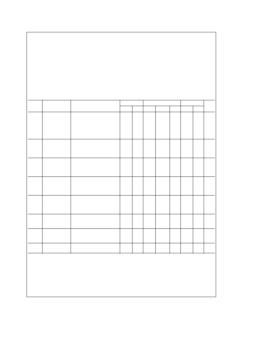
DC Electrical Characteristics
CD4070BM CD4077BM (Note 2)
Symbol
Parameter
Conditions
b
55 C
a
25 C
a
125 C
Units
Min
Max
Min
Typ
Max
Min
Max
I
DD
Quiescent Device
V
DD
e
5V
0 25
0 25
7 5
m
A
Current
V
IN
e
V
DD
or V
SS
V
DD
e
10V
0 5
0 5
15
m
A
V
IN
e
V
DD
or V
SS
V
DD
e
15V
1 0
1 0
30
m
A
V
IN
e
V
DD
or V
SS
V
OL
Low Level
l
I
O
l
k
1 mA
Output Voltage
V
DD
e
5V
0 05
0
0 05
0 05
V
V
DD
e
10V
0 05
0
0 05
0 05
V
V
DD
e
15V
0 05
0
0 05
0 05
V
V
OH
High Level
l
I
O
l
k
1 mA
Output Voltage
V
DD
e
5V
4 95
4 95
5
4 95
V
V
DD
e
10V
9 95
9 95
10
9 95
V
V
DD
e
15V
14 95
14 95
15
14 95
V
V
IL
Low Level
l
I
O
l
k
1 mA
Input Voltage
V
DD
e
5V V
O
e
4 5V or 0 5V
1 5
1 5
1 5
V
V
DD
e
10V V
O
e
9V or 1 0V
3 0
3 0
3 0
V
V
DD
e
15V V
O
e
13 5V or 1 5V
4 0
4 0
4 0
V
V
IH
High Level
l
I
O
l
k
1 mA
Input Voltage
V
DD
e
5V V
O
e
0 5V or 4 5V
3 5
3 5
3 5
V
V
DD
e
10V V
O
e
1 0V or 9 0V
7 0
7 0
7 0
V
V
DD
e
15V V
O
e
1 5V or 13 5V
11 0
11 0
11 0
V
I
OL
Low Level Output
V
DD
e
5V V
O
e
0 4V
0 64
0 51
0 88
0 36
mA
Current (Note 3)
V
DD
e
10V V
O
e
0 5V
1 6
1 3
2 25
0 9
mA
V
DD
e
15V V
O
e
1 5V
4 2
3 4
8 8
2 4
mA
I
OH
High Level Output
V
DD
e
5V V
O
e
4 6V
b
0 64
b
0 51
b
0 88
b
0 36
mA
Current (Note 3)
V
DD
e
10V V
O
e
9 5V
b
1 6
b
1 3
b
2 25
b
0 9
mA
V
DD
e
15V V
O
e
13 5V
b
4 2
b
3 4
b
8 8
b
2 4
mA
I
IN
Input Current
V
DD
e
15V V
IN
e
0V
b
0 1
b
10
b
5
b
0 1
b
1 0
m
A
V
DD
e
15V V
IN
e
15V
0 1
10
b
5
0 1
1 0
m
A
Note 1
``Absolute Maximum Ratings'' are those values beyond which the safety of the device cannot be guaranteed They are not meant to imply that the devices
should be operated at these limits The table of ``Recommended Operating Conditions'' and ``Electrical Characteristics'' provides conditions for actual device
operation
Note 2
V
SS
e
0V unless otherwise specified
Note 3
I
OL
and I
OH
are tested one output at a time
2
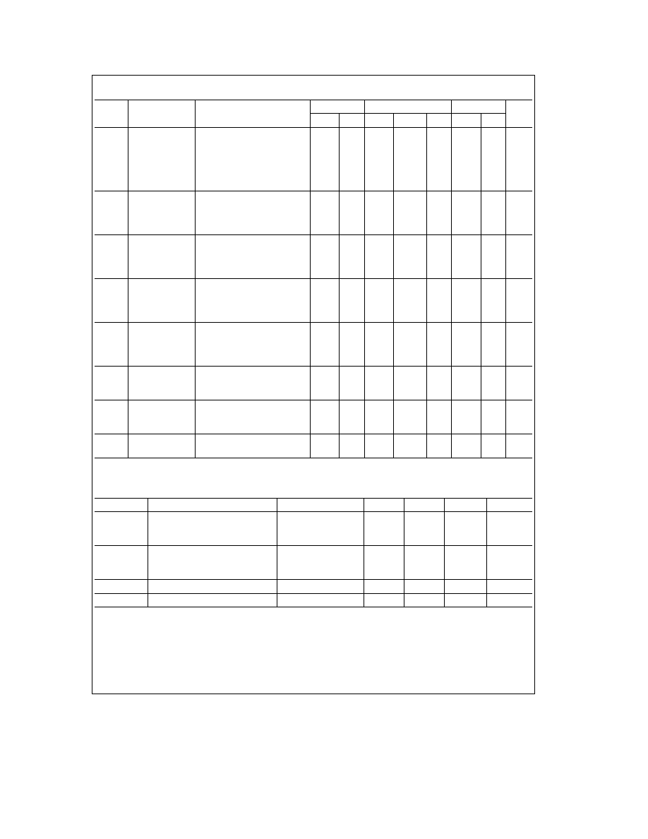
DC Electrical Characteristics
CD4070BC CD4077BC (Note 2)
Symbol
Parameter
Conditions
b
40 C
a
25 C
a
85 C
Units
Min
Max
Min
Typ
Max
Min
Max
I
DD
Quiescent Device
V
DD
e
5V
1 0
1 0
7 5
m
A
Current
V
IN
e
V
DD
or V
SS
V
DD
e
10V
2 0
2 0
15
m
A
V
IN
e
V
DD
or V
SS
V
DD
e
15V
4 0
4 0
30
m
A
V
IN
e
V
DD
or V
SS
V
OL
Low Level
l
I
O
l
k
1 mA
Output Voltage
V
DD
e
5V
0 05
0
0 05
0 05
V
V
DD
e
10V
0 05
0
0 05
0 05
V
V
DD
e
15V
0 05
0
0 05
0 05
V
V
OH
High Level
l
I
O
l
k
1 mA
Output Voltage
V
DD
e
5V
4 95
4 95
5
4 95
V
V
DD
e
10V
9 95
9 95
10
9 95
V
V
DD
e
15V
14 95
14 95
15
14 95
V
V
IL
Low Level
l
I
O
l
k
1 mA
Input Voltage
V
DD
e
5V V
O
e
4 5V or 0 5V
1 5
1 5
1 5
V
V
DD
e
10V V
O
e
9V or 1 0V
3 0
3 0
3 0
V
V
DD
e
15V V
O
e
13 5V or 1 5V
4 0
4 0
4 0
V
V
IH
High Level
l
I
O
l
k
1 mA
Input Voltage
V
DD
e
5V V
O
e
0 5V or 4 5V
3 5
3 5
3 5
V
V
DD
e
10V V
O
e
1V or 9 0V
7 0
7 0
7 0
V
V
DD
e
15V V
O
e
1 5V or 13 5V
11 0
11 0
11 0
V
I
OL
Low Level Output
V
DD
e
5V V
O
e
0 4V
0 52
0 44
0 88
0 36
mA
Current
V
DD
e
10V V
O
e
0 5V
1 3
1 1
2 25
0 9
mA
V
DD
e
15V V
O
e
1 5V
3 6
3 0
8 8
2 4
mA
I
OH
High Level Output
V
DD
e
5V V
O
e
4 6V
b
0 52
b
0 44
b
0 88
b
0 36
mA
Current
V
DD
e
10V V
O
e
9 5V
b
1 3
b
1 1
b
2 25
b
0 9
mA
V
DD
e
15V V
O
e
13 5V
b
3 6
b
3 0
b
8 8
b
2 4
mA
I
IN
Input Current
V
DD
e
15V V
IN
e
0V
b
0 3
b
10
b
5
b
0 3
b
1 0
m
A
V
DD
e
15V V
IN
e
15V
0 3
10
b
5
0 3
1 0
m
A
AC Electrical Characteristics
T
A
e
25 C C
L
e
50 pF R
L
e
200k t
r
and t
f
s
20 ns unless otherwise specified
Symbol
Parameter
Conditions
Min
Typ
Max
Units
t
PHL
or
Propagation Delay Time
V
DD
e
5V
110
185
ns
t
PLH
from Input to Output
V
DD
e
10V
50
90
ns
V
DD
e
15V
40
75
ns
t
THL
or
Transition Time
V
DD
e
5V
100
200
ns
t
TLH
V
DD
e
10V
50
100
ns
V
DD
e
15V
40
80
ns
C
IN
Average Input Capacitance
Any Input
5
7 5
pF
C
PD
Power Dissipation Capacitance
Any Input (Note 4)
20
pF
AC Parameters are guaranteed by DC correlated testing
Note 1
``Absolute Maximum Ratings'' are those values beyond which the safety of the device cannot be guaranteed They are not meant to imply that the devices
should be operated at these limits The table of ``Recommended Operating Conditions'' and ``Electrical Characteristics'' provides conditions for actual device
operation
Note 2
V
SS
e
0V unless otherwise specified
Note 3
I
OL
and I
OH
are tested one output at a time
Note 4
C
PD
determines the no load AC power consumption of any CMOS device For complete explanation see 54C 74C Family Characteristics Application
Note
AN-90
3
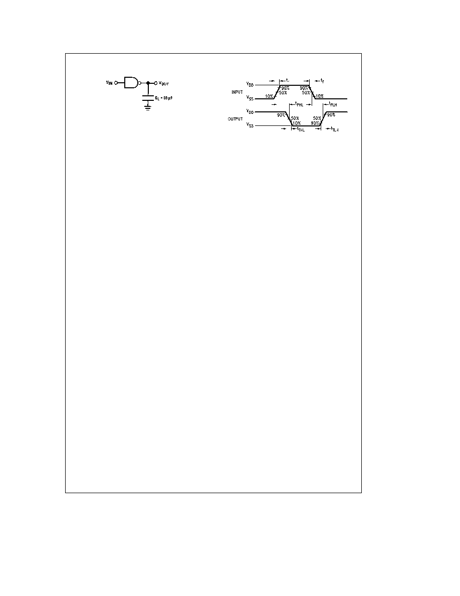
AC Test Circuit and Switching Time Waveforms
TL F 5976 � 3
Note
Delays measured with input t
r
t
f
e
20 ns
TL F 5976 � 4
t
r
e
t
f
e
20 ns
4
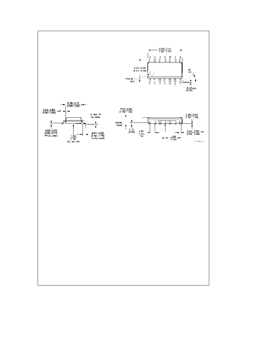
Physical Dimensions
inches (millimeters)
Molded Small Outline Package (M)
Order Number CD4070BCM or CD4077BCM
NS Package Number M14A
5
CD4070BMCD4070BCCD4077BMCD4077BC
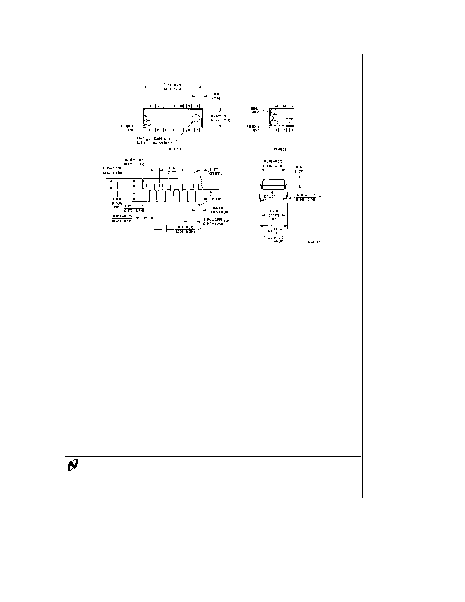
Physical Dimensions
inches (millimeters) (Continued)
Molded Dual-In-Line Package (N)
Order Number CD4070BCN or CD4077BCN
NS Package Number N14A
LIFE SUPPORT POLICY
NATIONAL'S PRODUCTS ARE NOT AUTHORIZED FOR USE AS CRITICAL COMPONENTS IN LIFE SUPPORT
DEVICES OR SYSTEMS WITHOUT THE EXPRESS WRITTEN APPROVAL OF THE PRESIDENT OF NATIONAL
SEMICONDUCTOR CORPORATION As used herein
1 Life support devices or systems are devices or
2 A critical component is any component of a life
systems which (a) are intended for surgical implant
support device or system whose failure to perform can
into the body or (b) support or sustain life and whose
be reasonably expected to cause the failure of the life
failure to perform when properly used in accordance
support device or system or to affect its safety or
with instructions for use provided in the labeling can
effectiveness
be reasonably expected to result in a significant injury
to the user
National Semiconductor
National Semiconductor
National Semiconductor
National Semiconductor
Corporation
Europe
Hong Kong Ltd
Japan Ltd
1111 West Bardin Road
Fax (a49) 0-180-530 85 86
13th Floor Straight Block
Tel 81-043-299-2309
Arlington TX 76017
Email cnjwge tevm2 nsc com
Ocean Centre 5 Canton Rd
Fax 81-043-299-2408
Tel 1(800) 272-9959
Deutsch Tel (a49) 0-180-530 85 85
Tsimshatsui Kowloon
Fax 1(800) 737-7018
English
Tel (a49) 0-180-532 78 32
Hong Kong
Fran ais Tel (a49) 0-180-532 93 58
Tel (852) 2737-1600
Italiano
Tel (a49) 0-180-534 16 80
Fax (852) 2736-9960
National does not assume any responsibility for use of any circuitry described no circuit patent licenses are implied and National reserves the right at any time without notice to change said circuitry and specifications