 | –≠–ª–µ–∫—Ç—Ä–æ–Ω–Ω—ã–π –∫–æ–º–ø–æ–Ω–µ–Ω—Ç: CD4503 | –°–∫–∞—á–∞—Ç—å:  PDF PDF  ZIP ZIP |
TL F 5989
CD4503BMCD4503BC
Hex
Non-Inverting
TRI-STATE
Buffer
October 1993
CD4503BM CD4503BC Hex
Non-Inverting TRI-STATE
Buffer
General Description
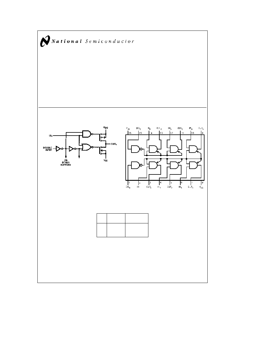
The CD4503B is a hex non-inverting TRI-STATE buffer with
high output current sink and source capability TRI-STATE
outputs make it useful in bus-oriented applications Two
separate disable inputs are provided Buffers 1 through 4
are controlled by the disable 4 input Buffers 5 and 6 are
controlled by the disable 2 input A high level on either dis-
able input will cause those gates on its control line to go into
a high impedance state
Features
Y
Wide supply voltage range
3 0 V
DC
to 18 V
DC
Y
TRI-STATE outputs
Y
Symmetrical turn on turn off delays
Y
Symmetrical output rise and fall times
Y
Pin-for-pin replacement for MM80C97 and MC14503
Schematic and Connection Diagrams
TL F 5989 ≠ 1
Dual-In-Line Package
TL F 5989 ≠ 2
Top View
Order Number CD4503B
Truth Table
In
Disable
Out
Input
0
0
0
1
0
1
X
1
TRI-STATE
X
e
Don't Care
TRI-STATE
is a registered trademark of National Semiconductor Corporation
C1995 National Semiconductor Corporation
RRD-B30M105 Printed in U S A

Absolute Maximum Ratings
(Notes 1 and 2)
If Military Aerospace specified devices are required
please contact the National Semiconductor Sales
Office Distributors for availability and specifications
Supply Voltage (V
DD
)
b
0 5V to
a
18V
Input Voltage (V
IN
)
b
0 5V to
a
0 5V
Storage Temperature Range (T
S
)
b
65 C to
a
150 C
Power Dissipation (P
D
)
Dual-In-Line
700 mW
Small Outline
500 mW
Lead Temperature (T
L
)
(Soldering 10 seconds)
260 C
Recommended Operating
Conditions
(Note 2)
Supply Voltage (V
DD
)
a
3V to
a
15V
Operating Temperature Range (T
A
)
CD4503BM
b
55 C to
a
125 C
CD4503BC
b
40 C to
a
85 C
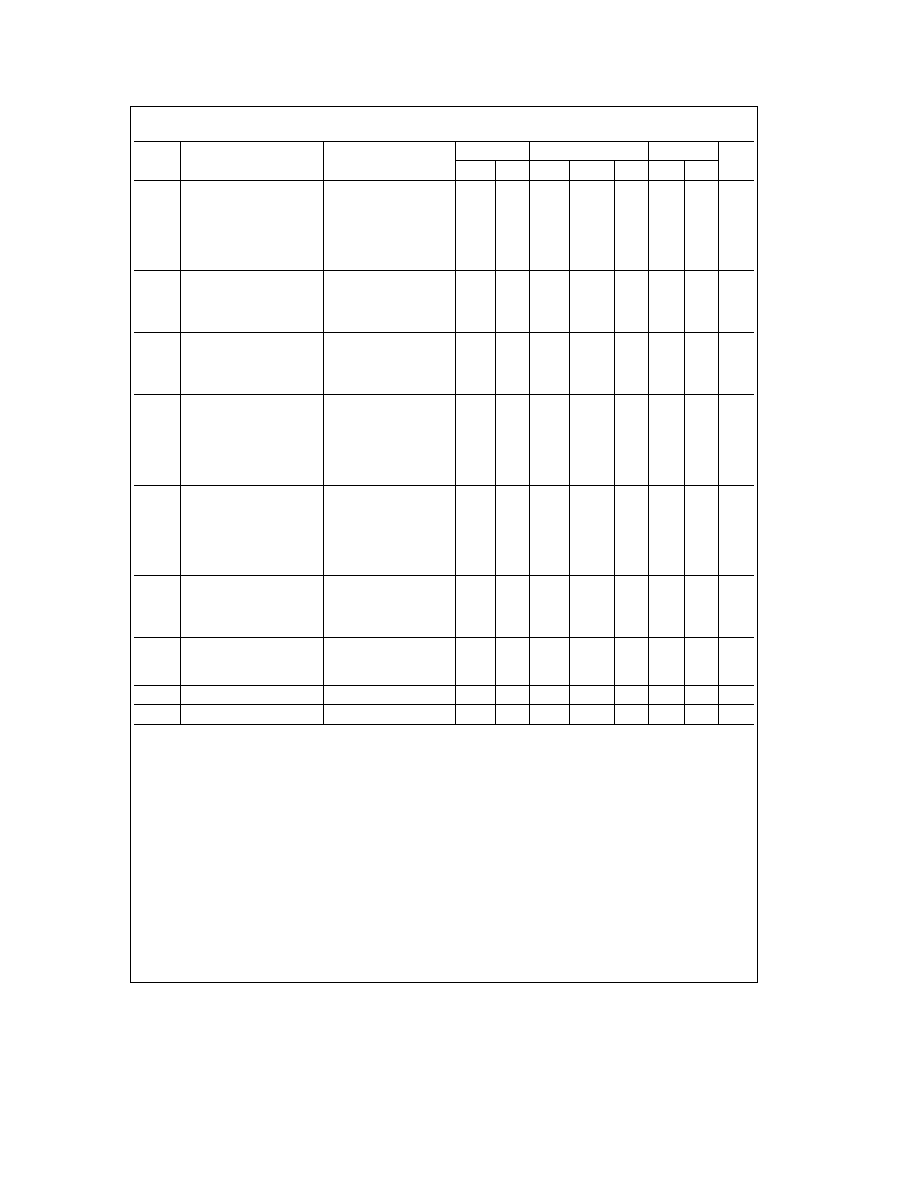
DC Electrical Characteristics
CD4503BM (Note 2)
Symbol
Parameter
Conditions
b
55 C
a
25
a
125 C
Units
Min
Max
Min
Typ
Max
Min
Max
I
DD
Quiescent Device
V
DD
e
5V
1
1
30
m
A
Current
V
IN
e
V
DD
or V
SS
V
DD
e
10V
2
2
60
m
A
V
IN
e
V
DD
or V
SS
V
DD
e
15V
4
4
120
m
A
V
IN
e
V
DD
or V
SS
V
OL
Low Level
V
IN
e
V
DD
or 0
Output Voltage
V
DD
e
5V
0 05
0
0 05
0 05
V
V
DD
e
10V
0 05
0
0 05
0 05
V
V
DD
e
15V
0 05
0
0 05
0 05
V
V
OH
High Level
V
IN
e
V
DD
or 0
Output Voltage
V
DD
e
5V
4 95
4 95
5
4 95
V
V
DD
e
10V
9 95
9 95
10
9 95
V
V
DD
e
15V
14 95
14 95
15
14 95
V
V
IL
Low Level
V
DD
e
5V
1 5
2 25
1 5
1 5
V
Input Voltage
V
O
e
4 5V or 0 5V
V
DD
e
10V
3 0
4 50
3 0
3 0
V
V
O
e
9 0V or 1 0V
V
DD
e
15V
4 0
6 75
4 0
4 0
V
V
O
e
13 5V or 1 5V
V
IH
High Level
V
DD
e
5V
3 5
3 5
2 75
3 5
V
Input Voltage
V
O
e
0 5V or 4 5V
V
DD
e
10V
7 0
7 0
5 5
7 0
V
V
O
e
1 0V or 9 0V
V
DD
e
15V
11 0
11 0
8 25
11 0
V
V
O
e
1 5V or 13 5V
I
OL
Low Level Output
V
DD
e
4 5V V
OL
e
0 4V
2 80
2 30
2 55
1 60
mA
Current (Note 3)
V
DD
e
5 0V V
OL
e
0 4V
3 00
2 40
2 75
1 75
mA
V
DD
e
10V V
OL
e
0 5V
7 85
6 35
7 00
4 45
mA
V
DD
e
15V V
OL
e
1 5V
19 95
16 10
25 00
11 30
mA
I
OH
High Level Output
V
DD
e
5V V
OH
e
4 6V
b
1 28
b
1 02
b
1 76
b
0 72
mA
Current (Note 3)
V
DD
e
10V V
OH
e
9 5V
b
3 20
b
2 60
b
4 5
b
1 8
mA
V
DD
e
15V V
OH
e
13 5V
b
8 20
b
6 80
b
17 6
b
4 8
mA
I
OZ
TRI-STATE Leakage Current V
DD
e
15V
g
0 1
g
10
b
4
g
0 1
g
1 0
m
A
I
IN
Input Current
V
DD
e
15V
g
0 1
g
10
b
4
g
0 1
g
1 0
m
A
Note 1
``Absolute Maximum Ratings'' are those values beyond which the safety of the device cannot be guaranteed They are not meant to imply that the devices
should be operated at these limits The tables of ``Recommended Operating Conditions'' and ``Electrical Characteristics'' provide conditions for actual device
operation
Note 2
V
SS
e
0V unless otherwise specified
Note 3
I
OH
and I
OL
are tested one output at a time
2
DC Electrical Characteristics
CD4503BC (Note 2)
Symbol
Parameter
Conditions
b
40 C
a
25 C
a
85 C
Units
Min
Max
Min
Typ
Max
Min
Max
I
DD
Quiescent Device
V
DD
e
5V
4
4
30
m
A
Current
V
IN
e
V
DD
or V
SS
V
DD
e
10V
8
8
60
m
A
V
IN
e
V
DD
or V
SS
V
DD
e
15V
16
16
120
m
A
V
IN
e
V
DD
or V
SS
V
OL
Low Level
V
IN
e
V
DD
or 0
Output Voltage
V
DD
e
5V
0 05
0
0 05
0 05
V
V
DD
e
10V
0 05
0
0 05
0 05
V
V
DD
e
15V
0 05
0
0 05
0 05
V
V
OH
High Level
V
IN
e
V
DD
or 0
Output Voltage
V
DD
e
5V
4 95
4 95
4 95
V
V
DD
e
10V
9 95
9 95
9 95
V
V
DD
e
15V
14 95
14 95
14 95
V
V
IL
Low Level
V
DD
e
5V
1 5
2 25
1 5
1 5
V
Input Voltage
V
O
e
4 5V or 0 5V
V
DD
e
10V
3 0
4 50
3 0
3 0
V
V
O
e
9 0V or 1 0V
V
DD
e
15V
4 0
6 75
4 0
4 0
V
V
O
e
13 5V or 1 5V
V
IH
High Level
V
DD
e
5V
3 5
3 5
2 75
3 5
V
Input Voltage
V
O
e
0 5V or 4 5V
V
DD
e
10V
7 0
7 0
5 5
7 0
V
V
O
e
1 0V or 9 0V
V
DD
e
15V
11 0
11 0
8 25
11 0
V
V
O
e
1 5V or 13 5V
I
OL
Low Level Output
V
DD
e
4 5V V
OL
e
0 4V
2 30
1 95
2 65
1 60
mA
Current (Note 3)
V
DD
e
5 0V V
OL
e
0 4V
2 5
2 10
2 75
1 75
mA
V
DD
e
10V V
OL
e
0 5V
6 5
5 45
7 0
4 45
mA
V
DD
e
15V V
OL
e
1 5V
16 50
13 80
25 00
11 30
mA
I
OH
High Level Output
V
DD
e
5V V
OH
e
4 6V
b
1 04
b
0 88
b
1 76
b
0 7
mA
Current (Note 3)
V
DD
e
10V V
OH
e
9 5V
b
2 60
b
2 2
b
4 50
b
1 8
mA
V
DD
e
15V V
OH
e
13 5V
b
7 2
b
6 0
b
17 6
b
4 8
mA
I
TL
TRI-STATE Leakage Current V
DD
e
15V
g
0 3
g
10
b
4
g
0 3
g
1 0
m
A
I
IN
Input Current
V
DD
e
15V
g
0 3
g
10
b
5
g
0 3
g
1 0
m
A
Note 1
``Absolute Maximum Ratings'' are those values beyond which the safety of the device cannot be guaranteed They are not meant to imply that the devices
should be operated at these limits The tables of ``Recommended Operating Conditions'' and ``Electrical Characteristics'' provide conditions for actual device
operation
Note 2
V
SS
e
0V unless otherwise specified
3
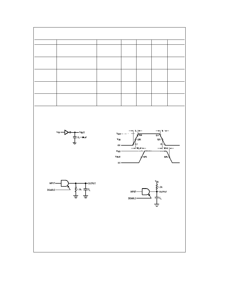
AC Electrical Characteristics
CD4503B
T
A
e
25 C C
L
e
50 pF R
L
e
200 kX Input t
r
e
t
f
e
20 ns unless otherwise specified
Symbol
Parameter
Conditions
Min
Typ
Max
Units
t
PHL
t
PLH
Propagation Delay Time
V
DD
e
5V
75
100
ns
V
DD
e
10V
35
40
ns
V
DD
e
15V
25
30
ns
t
PLZ
t
PHZ
Propagation Delay Time
V
DD
e
5V
80
125
ns
Logical Level to High
V
DD
e
10V
40
90
ns
Impedance State
V
DD
e
15V
35
70
ns
t
PZL
t
PZH
Propagation Delay Time
V
DD
e
5V
95
175
ns
High Impedance State to
V
DD
e
10V
40
80
ns
Logical Level
V
DD
e
15V
35
70
ns
t
TLH
Output Rise Time
V
DD
e
5V
45
80
ns
V
DD
e
10V
23
40
ns
V
DD
e
15V
18
35
ns
t
THL
Output Fall Time
V
DD
e
5V
45
80
ns
V
DD
e
10V
23
40
ns
V
DD
e
15V
18
35
ns
AC Parameters are guaranteed by DC correlated testing
AC Test Circuits and Switching Time Waveforms
t
PHL
t
PLH
TL F 5989 ≠ 3
CMOS to CMOS
TL F 5989 ≠ 4
t
PHZ
and t
PZH
TL F 5989 ≠ 5
t
PLZ
and t
PZL
TL F 5989 ≠ 6
4
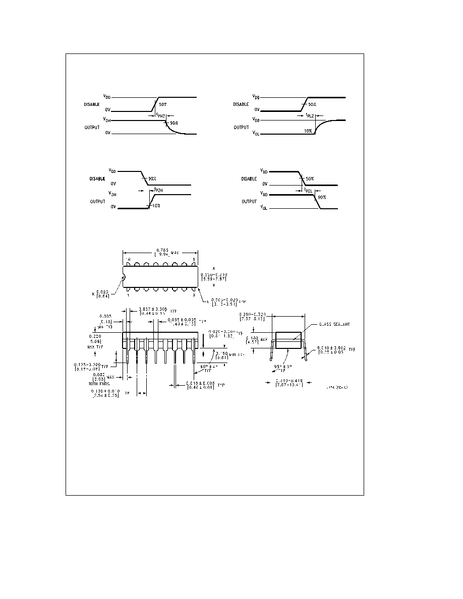
AC Test Circuits and Switching Time Waveforms
(Continued)
t
PHZ
TL F 5989 ≠ 7
t
PLZ
TL F 5989 ≠ 8
t
PZH
TL F 5989 ≠ 9
Note
Delays measured with input t
r
t
f
s
20 ns
t
PZL
TL F 5989 ≠ 10
Physical Dimensions
inches (millimeters)
Ceramic Dual-In-Line Package (J)
Order Number CD4503BMJ or CD4503BCJ
NS Package Number J16A
5