TL F 10966
CGS74B303
Octal
Divide-by-2
Skew
Clock
Driver
July 1996
CGS74B303 Octal Divide-by-2 Skew Clock Driver
General Description
These minimum skew clock drivers are designed for high
frequency Clock Generation and Support (CGS) applica-
tions These devices are ideal for duty cycle recovery appli-
cations with internal frequency divide-by-2 circuitry The de-
vices guarantee minimum skew across the outputs of a giv-
en device Skew parameters are also provided as a means
to measure duty cycle requirements as those found in high
speed clocking systems
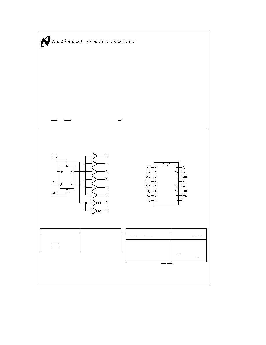
Functional Description
The CGS74B303 contains eight flip-flops designed to have
low skew between outputs The eight outputs (six in-phase
with CLK and two out-of-phase) toggle on successive CLK
pulses PRE and CLR inputs are provided to set Q and Q
outputs high or low independent of CLK pin
Features
Y
Clock Generation and Support (CGS) Devices ideal for
high frequency signal generation or clock distribution
applications
Y
Fabricated on National's Advanced Bipolar FAST
TM
LSl
process
Y
1 ns pin-to-pin output skew
Y
Specification for transition skew to meet duty cycle
requirements
Y
Current sourcing 24 mA and current sinking of 48 mA
Y
Low dynamic power consumption above 20 MHz
Y
Guaranteed 4 kV ESD protection
Logic Diagram
Connection Diagram
TL F 10966 ≠ 3
Pin Assignment
SOlC (M)
TL F 10966 ≠ 1
Pin Description
Pin Names
Description
CLK
Clock Input
Q
0
≠ Q
7
Outputs
PRE
Preset
CLR
Clear
Truth Table
Inputs
Outputs
CLR
PRE
CLK
Q
0
≠ Q
5
Q
6
≠ Q
7
L
H
X
L
H
H
L
X
H
L
L
L
X
L
L
H
H
u
Q
Q
H
H
L
Q
Q
This state will not persist when CLR PRE returns to high
TRI-STATE
is a registered trademark of National Semiconductor Corporation
FAST
TM
is a trademark of National Semiconductor Corporation
C1996 National Semiconductor Corporation
RRD-B30M86 Printed in U S A
http
www national com
Absolute Maximum Ratings
(Note)
If Military Aerospace specified devices are required
please contact the National Semiconductor Sales
Office Distributors for availability and specifications
Supply Voltage (V
CC
)
7 0V
Input Voltage (V
I
)
7 0V
Operating Free Air Temperature
0 C to
a
70 C
Storage Temperature Range
b
65 C to
a
150 C
Typical i
JA
Airflow (LFM)
0
225
500
Jedec SOIC (M) Package
118
96
86
C W
Recommended Operating
Conditions
Supply Voltage (V
CC
)
4 5V to 5 5V
Input Rise and Fall Times
2 ns max
(0 8V to 2 0V)
Free Air Operating Temperature (T
A
)
0 C to 70 C
NOTE
The Absolute Maximum Ratings are those values
beyond which the safety of the device cannot be guaran-
teed The device should not be operated at these limits The
parametric values defined in the DC and AC Electrical Char-
acteristics tables are not guaranteed at the absolute maxi-
mum ratings The Recommended Operating Conditions will
define the conditions for actual device operation
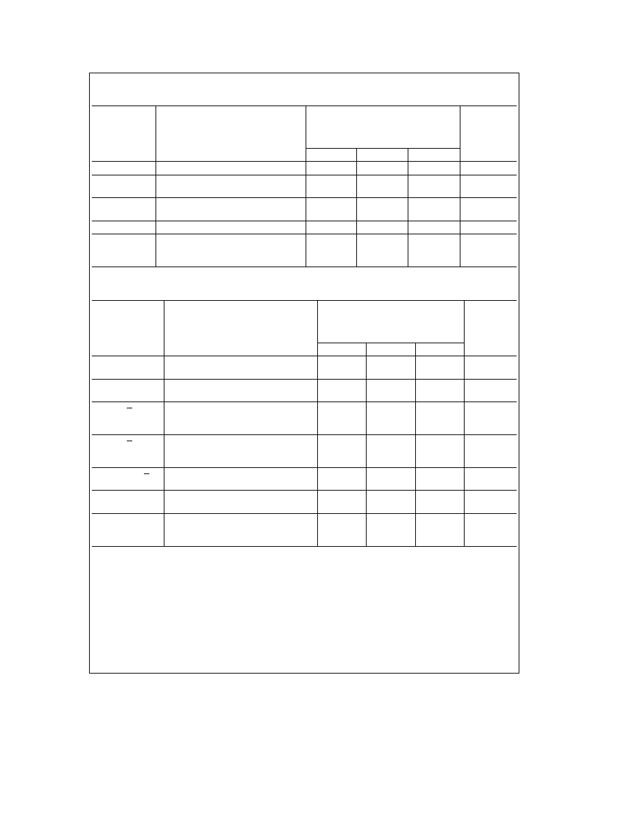
DC Electrical Characteristics
Over recommended operating conditions unless specified otherwise All typical values are measured at V
CC
e
5V T
A
e
25 C
Symbol
Parameter
Conditions
Min
Typ
Max
Unit
V
IK
Input Clamp Voltage
V
CC
e
4 5V I
I
e b
18 mA
b
1 2
V
V
IH
Minimum Input
2 0
V
High Level Voltage
V
IL
Maximum Input
0 8
V
Low Level Voltage
V
OH
High Level Output Voltage
I
OH
e b
2 mA V
CC
e
4 5V
V
CC
b
2
V
I
OH
e b
24 mA V
CC
e
4 5V
2 0
V
OL
Low Level Output Voltage
V
CC
e
4 5V I
OL
e
48 mA
0 35
0 5
V
I
I
Input Current
Max
V
CC
e
5 5V V
IH
e
7V
0 1
m A
Input Voltage
I
IH
High Level Input Current
V
CC
e
5 5V V
IH
e
2 7V
20
m
A
I
IL
Low Level Input Current
V
CC
e
5 5V V
IL
e
0 4V
b
0 1
b
0 50
mA
I
O
Output Drive Current
V
CC
e
5 5V V
O
e
2 25V
b
50
b
150
mA
I
CC
Supply Current
V
CC
e
5 5V
Outputs High
27
60
mA
Outputs Low
45
60
mA
C
IN
Input Capacitance
V
CC
e
5V
5
pF
http
www national com
2
AC Electrical Characteristics
Over recommended operating conditions unless specified otherwise All typical values are measured at V
CC
e
5V T
A
e
25 C
V
CC
e
4 5V to 5 5V
T
A
e
0 C to
a
70 C
Symbol
Parameter
C
L
e
0 pF ≠ 50 pF
Units
R
L
e
500X
Min
Typ
Max
f
MAX
Maximum Input Frequency (Note 2)
110
MHz
t
PLH
Propagation Delay CLKn to O
n
4
8 5
ns
t
PHL
(Note 2)
t
PLH
Propagation Delay PRE CLR
4
11
ns
t
PHL
t
SU
Set Up Time before CLK
5
ns
t
W
CLK HI
4
CLK LO
4
ns
CLR PRE
4
Extended AC Electrical Characteristics
Over recommended operating conditions unless specified otherwise All typical values are measured at V
CC
e
5V T
A
e
25 C
V
CC
e
4 5V to 5 5V
T
A
e
0 C to
a
70 C
Symbol
Parameter
C
L
e
0 pF ≠ 50 pF
Units
R
L
e
500X
Min
Typ
Max
t
OSHL Q
Maximum Skew Common Edge
0 5
1 0
ns
Output-to-Output Variation (Notes 1 2)
t
OSLH Q
Maximum Skew Common Edge
0 5
1 0
ns
Output-to-Output Variation (Notes 1 2)
t
OSHL Q
Maximum Skew Common Edge
Output-to-Output Variation
0 3
0 75
ns
(Notes 1 2)
t
OSLH Q
Maximum Skew Common Edge
Output-to-Output Variation
0 3
0 75
ns
(Notes 1 2)
t
OSLH HL Q Q
Maximum Skew Common Edge
1 0
1 6
ns
Output-to-Output Variation (Notes 1 2)
t
PS Q
Maximum Skew Pin (Signal)
1 0
ns
Transition Variation (Notes 1 2)
t
rise
Rise Fall Time
1 1
2 0
t
fall
(from 0 8V 2 0V to 2 0V 0 8V)
0 9
2 0
ns
0 pF ≠ 30 pF Loads
Note 1
Output-to-Output Skew is defined as the absolute value of the difference between the actual propagation delay for any outputs within the same packaged
device The specifications apply to any outputs switching in the same direction either HIGH to LOW (t
OSHL
) or LOW to HIGH (t
OSLH
) or in opposite directions both
HL and LH (t
OST
) Parameters t
OST
and t
PS
guaranteed by design
Note 2
This device is sensitive to noise due to the large transient currents which occur during multiple switching of the eight outptus V
CC
by-pass capacitor(s)
chip types must be placed as closely as possible to the V
CC
pin
Note 3
Refer to Minimum Skew Parameters Measurement Information Chart for definitions of each skew specification
Note 4
All input pulses are from 3 5V to 0 3V with rise and fall times of 2 0 ns
Note 5
Load capacitance includes the test jig
http
www national com
3
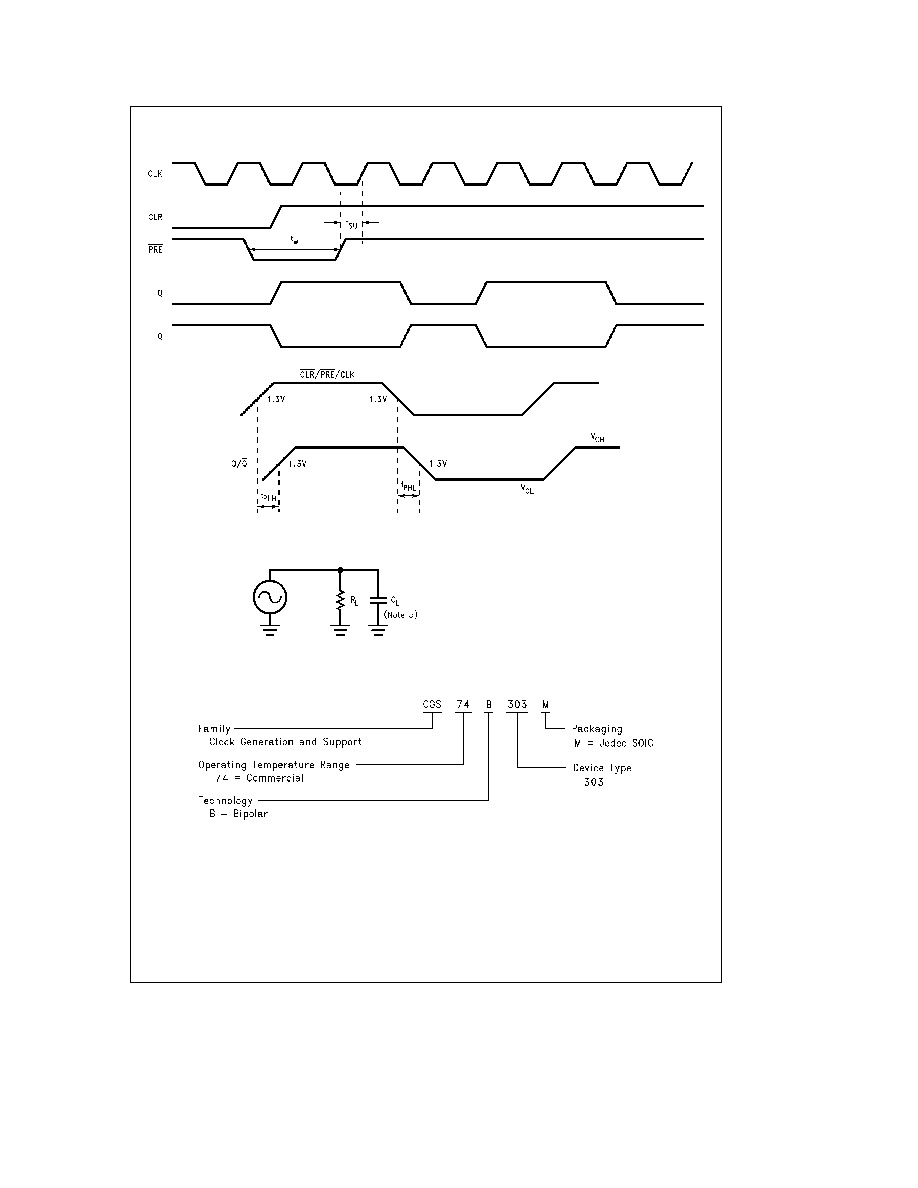
Timing Diagrams
Minimum Skew Divide-by-2 Clock Drivers
TL F 10966 ≠ 4
TL F 10966 ≠ 5
Test Circuit
TL F 10966 ≠ 6
R
L
is 500X
C
L
is 50 pF for all prop delays and skew measurements
C
L
is 30 pF for t
rise
and t
fall
measurements
Ordering Information
Contact NSC Marketing for specific date of availability
TL F 10966 ≠ 7
http
www national com
4

http
www national com
5