TL F 11752
CGS74CT2524
1
t
o
4
Minimum
Skew
(300
ps)
Clock
Driver
September 1995
CGS74CT2524
1 to 4 Minimum Skew (300 ps) Clock Driver
General Description
These minimum skew clock drivers are designed for Clock
Generation and Support (CGS) applications operating at
high frequencies This device guarantees minimum output
skew across the outputs of a given device
Skew parameters are also provided as a means to measure
duty cycle requirements as those found in high speed clock-
ing systems The CGS74CT2524 is a minimum skew clock
driver with one input driving four outputs specifically de-
signed for signal generation and clock distribution applica-
tions
Features
Y
Guaranteed 300 ps pin-to-pin skew (t
OSHL
and t
OSLH
)
Y
Implemented on National's FACT
TM
family process
Y
1 input to 4 outputs low skew clock distribution
Y
Symmetric output current drive 24 mA I
OH
I
OL
Y
Industrial temperature of
b
40 C to
a
85 C
Y
8-pin SOIC package
Y
Low dynamic power consumption above 20 MHz
Y
Guaranteed 2 kV ESD protection
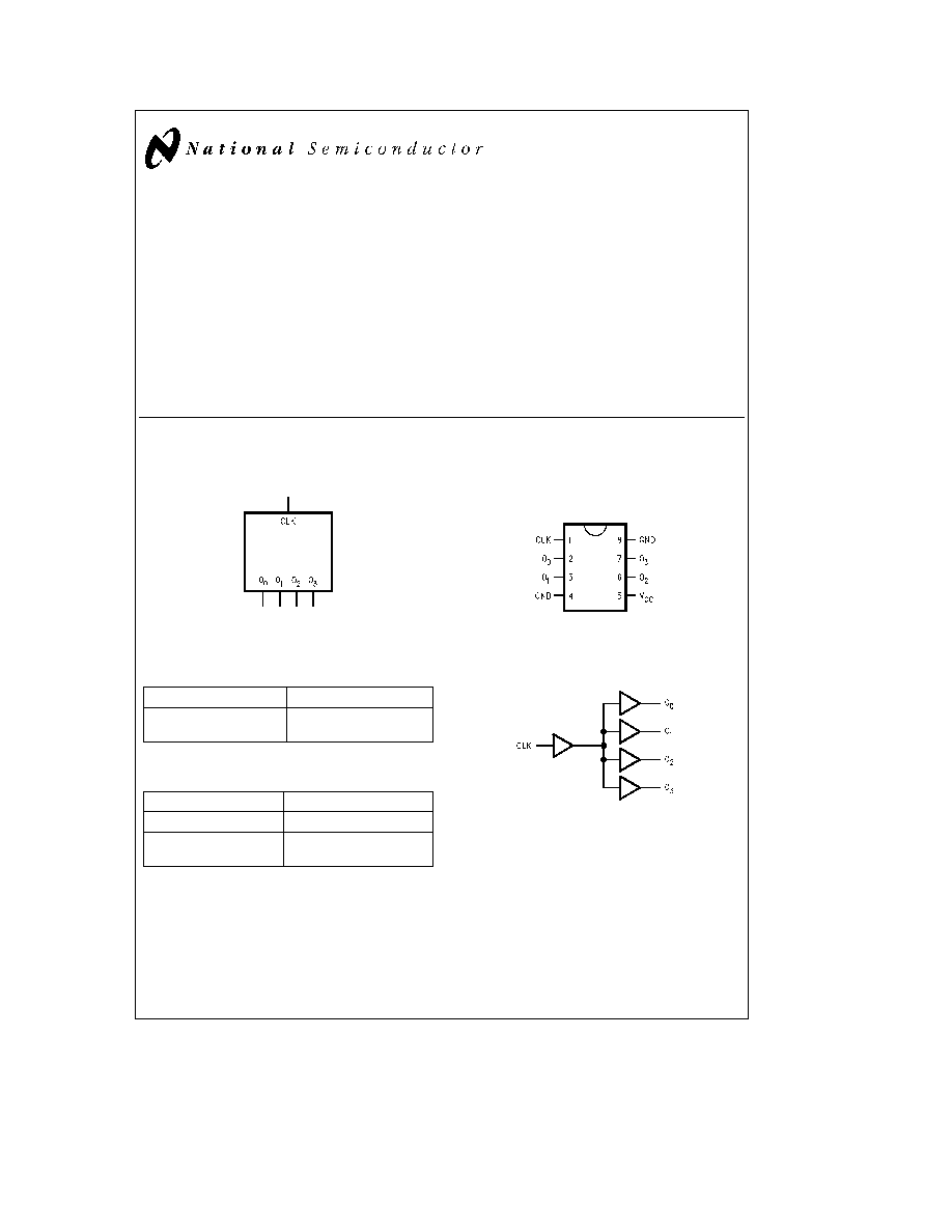
Logic Symbol
TL F 11752 ≠ 1
The output pins act as a single entity and will follow the state of the CLK
when the clock distribution chip is selected
Pin Description
Pin Names
Descripton
CLK
Clock Input
O
0
≠ O
3
Outputs
Truth Table
Inputs
Outputs
CLK
O
0
≠ O
3
L
L
H
H
L
e
Low Logic Level
H
e
High Logic Level
Connection Diagrams
Pin Assignment
SOIC (M)
TL F 11752 ≠ 2
TL F 11752 ≠ 3
FACT
TM
is a trademark of National Semiconductor Corporation
C1995 National Semiconductor Corporation
RRD-B30M115 Printed in U S A
Absolute Maximum Ratings
(Note)
If Military Aerospace specified devices are required
please contact the National Semiconductor Sales
Office Distributors for availability and specifications
Supply Voltage (V
CC
)
b
0 5 to 7 0V
DC Input Voltage Diode Current (I
IK
)
V
e b
0 5V
b
20 mA
V
e
V
CC
a
0 5V
a
20 mA
DC Input Voltage (V
I
)
b
0 5V to (V
CC
a
0 5V)
DC Output Diode (Current) (I
O
)
V
e b
0 5V
b
20 mA
V
e
V
CC
a
0 5V
a
20 mA
DC Output Voltage (V
O
)
b
0 5V to (V
CC
a
0 5V)
DC Output Source
or Sink Current (I
O
)
g
50 mA
DC V
CC
or Ground Current
per Output Pin (I
CC
or I
GND
)
g
50 mA
Storage Temperature (T
STG
)
b
65 C to
a
150 C
Junction Temperature (i
JA
)
0
225
500 LFM
M
167
132
117 C W
N
115
79
62 C W
Recommended Operating
Conditions
Supply Voltage (V
CC
)
4 5V to 5 5V
Input Voltage (V
I
)
0V to V
CC
Output Voltage (V
O
)
0 to V
CC
Operating Temperature (T
A
)
b
40 C to
a
85 C
Input Rise and Fall Times
(0 8V to 2 0V)
9 6 ns max
NOTE
The Absolute Maximum Ratings are those values
beyond which the safety of the device cannot be guaran-
teed The device should not be operated at these limits The
parametric values defined in the DC and AC Electrical Char-
acteristics tables are not guaranteed at the absolute maxi-
mum ratings The Recommended Operating Conditions will
define the conditions for actual device operation
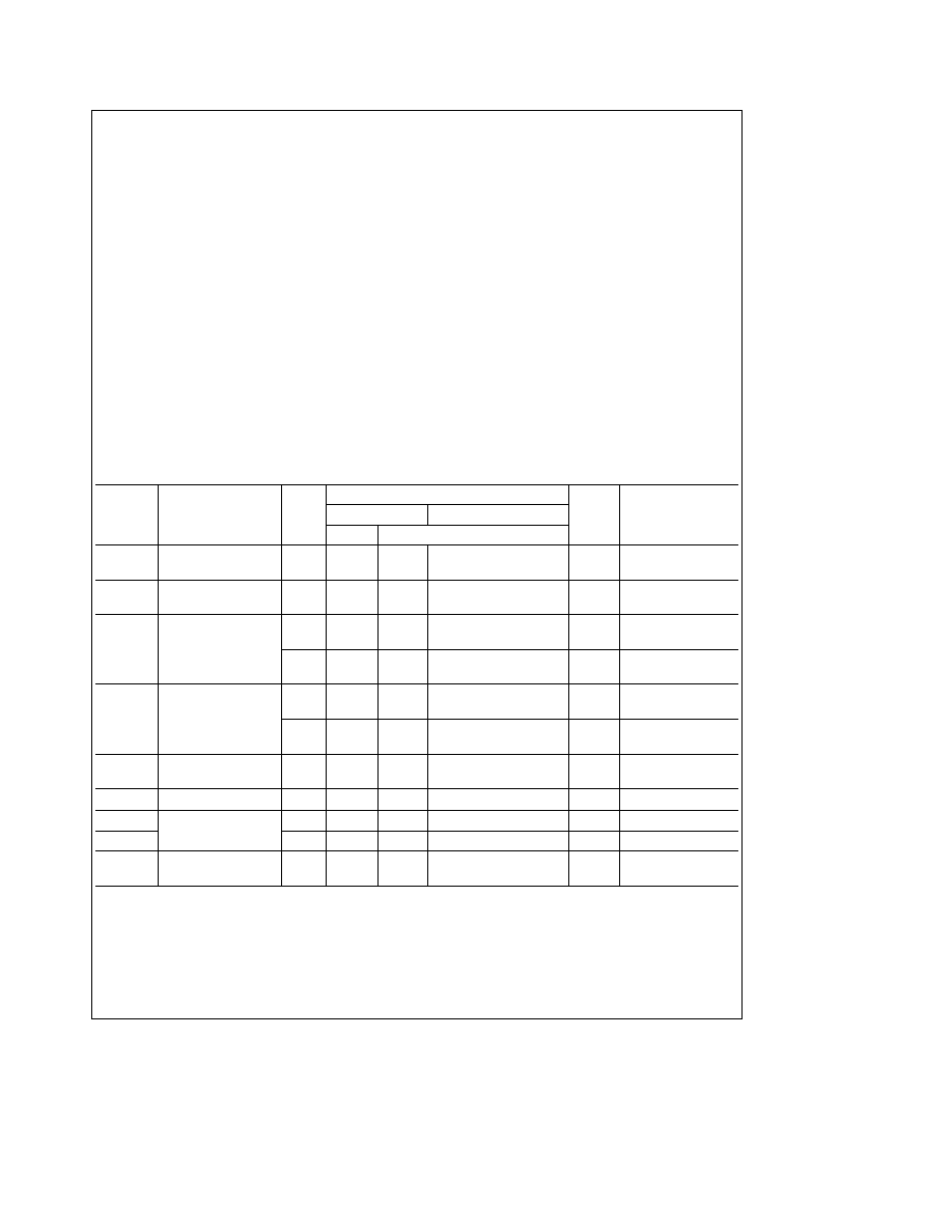
DC Electrical Characteristics
Over recommended operating conditions unless specified otherwise
Symbol
Parameter
V
CC
(V)
CGS74CT2524
Units
Conditions
T
A
e a
25 C
T
A
e b
40 C to
a
85 C
Typ
Guaranteed Limits
V
IH
Minimum High Level
4 5
1 5
2 0
2 0
V
V
OUT
e
0 1V
Input Voltage
5 5
1 5
2 0
2 0
or V
CC
e b
0 1V
V
IL
Maximum Low Level
4 5
1 5
0 8
0 8
V
V
OUT
e
0 1V
Input Voltage
5 5
1 5
0 8
0 8
or V
CC
e b
0 1V
V
OH
Minimum High Level
4 5
4 49
4 4
4 4
V
V
IN
e
V
IH
Output Voltage
5 5
5 49
5 4
5 4
I
OUT
e b
50 mA
4 5
3 86
3 76
V
V
IN
e
V
IH
5 5
4 86
4 76
I
OH
e b
24 mA
V
OL
Minimum Low Level
4 5
0 001
0 1
0 1
V
V
IN
e
V
IL
Output Voltage
5 5
0 001
0 1
0 1
I
OUT
e
50 mA
4 5
0 36
0 44
V
V
IN
e
V
IL
5 5
0 36
0 44
I
OL
e
24 mA
I
IN
Maximum Input
5 5
g
0 1
g
1 0
mA
V
I
e
V
CC
GND
Leakage Current
I
CCT
Maximum I
CC
Input
5 5
0 6
1 5
mA
V
I
e
V
CC
b
2 1V
I
OLD
Minimum Dynamic
5 5
75
mA
V
OLD
e
1 65V Max
I
OHD
Output Current
5 5
b
75
mA
V
OHD
e
3 85V Min
I
CC
Maximum Quiescent
5 5
8 0
80
m
A
V
IN
e
V
CC
Supply Current
or GND
2
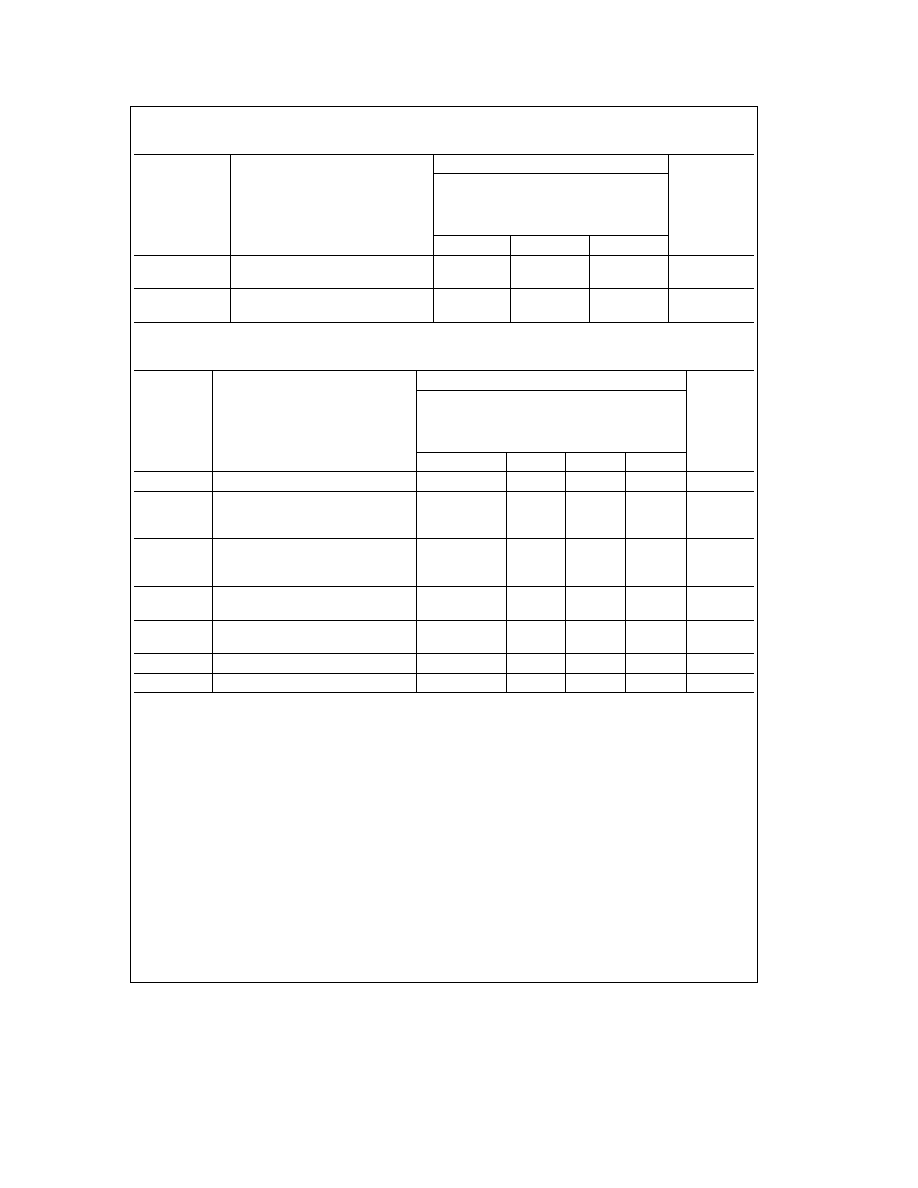
AC Electrical Characteristics
Over recommended operating conditions unless specified otherwise All typical values are measured at V
CC
e
5V T
A
e
25 C
Symbol
Parameter
CGS74CT2524
Units
V
CC
e
4 5V to 5 5V
T
A
e b
40 C to
a
85 C
C
L
e
50 pF
R
L
e
500X
Min
Typ
Max
t
PLH
Low-to-High Propagation Delay
3 5
9 0
ns
CLK to O
n
t
PHL
High-to-Low Propagation Delay
3 5
9 0
ns
CLK to O
n
Extended AC Electrical Characteristics
Over recommended operating conditions unless specified otherwise All typical values are measured at V
CC
e
5V T
A
e
25 C
Symbol
Parameter
CGS74CT2524
Units
V
CC
e
4 5V to 5 5V
T
A
e b
40 C to
a
85 C
C
L
e
50 pF
R
L
e
500X
Package
Min
Typ
Max
F
max
Maximum Operating Frequency
100
MHz
t
OSHL
Maximum Skew Common Edge
M
300
Output-to-Output Variation (Note 1)
M (Note 2)
450
ps
N
500
t
OSLH
Maximum Skew Common Edge
M
300
Output-to-Output Variation (Note 1)
M (Note 2)
450
ps
N
500
t
PS
Maximum Skew Pin (Signal)
1 0
ns
Transition Variation (Note 3)
t
rise
Rise Time Fall Time
1 5
ns
t
fall
(from 0 8V to 2 0V 2 0V to 0 8V)
T
High
Time High
4
ns
T
Low
Time Low
4
ns
Note 1
Output-to-Output Skew is defined as the absolute value of the difference between the actual propagation delay from any outputs within the same packaged
device The specifications apply to any outputs switching in the same direction either HIGH to LOW (t
OSHL
) or LOW to HIGH (t
OSLH
) or in opposite directions both
HL and LH (t
OST
) t
OSHL
and t
OSLH
are characterized and guaranteed by design
1 MHz
Note 2
Characterized at 66 MHz Parameter guaranteed by design
Note 3
Pin transition skew is the absolute difference between High-to-Low and Low-to-High propagation delay measure at a given output pin
Note 4
Load capacitance includes the test jig
3
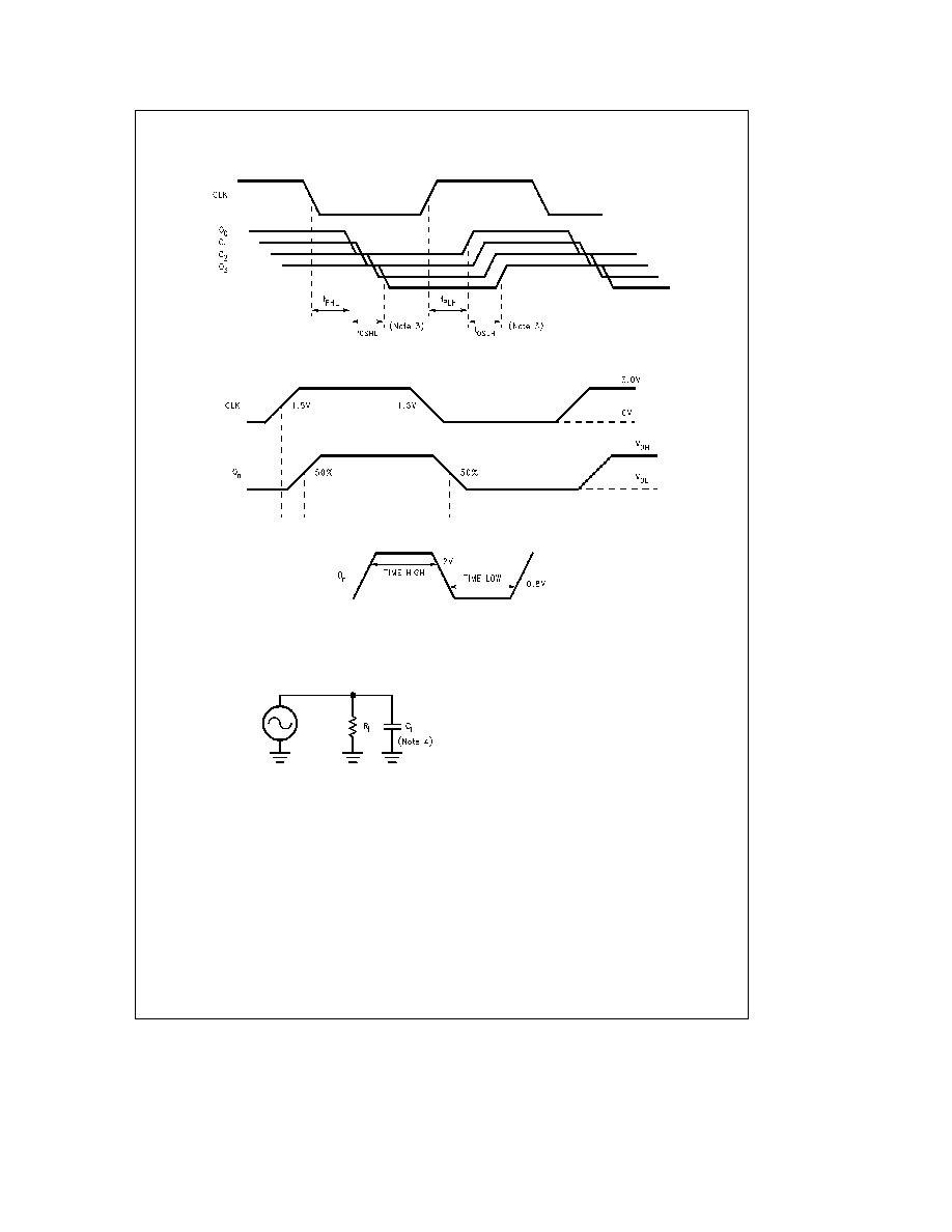
Timing Diagrams
1 to 4 Min-Skew Clock Driver
TL F 11752 ≠ 4
TL F 11752 ≠ 5
TL F 11752 ≠ 13
Time high is measured with outputs above 2V
Time low is measured with outputs below 0 8V
Test Circuit
TL F 11752 ≠ 6
R
L
is 500X
C
L
is 50 pF for all prop delays and skew measurements
4
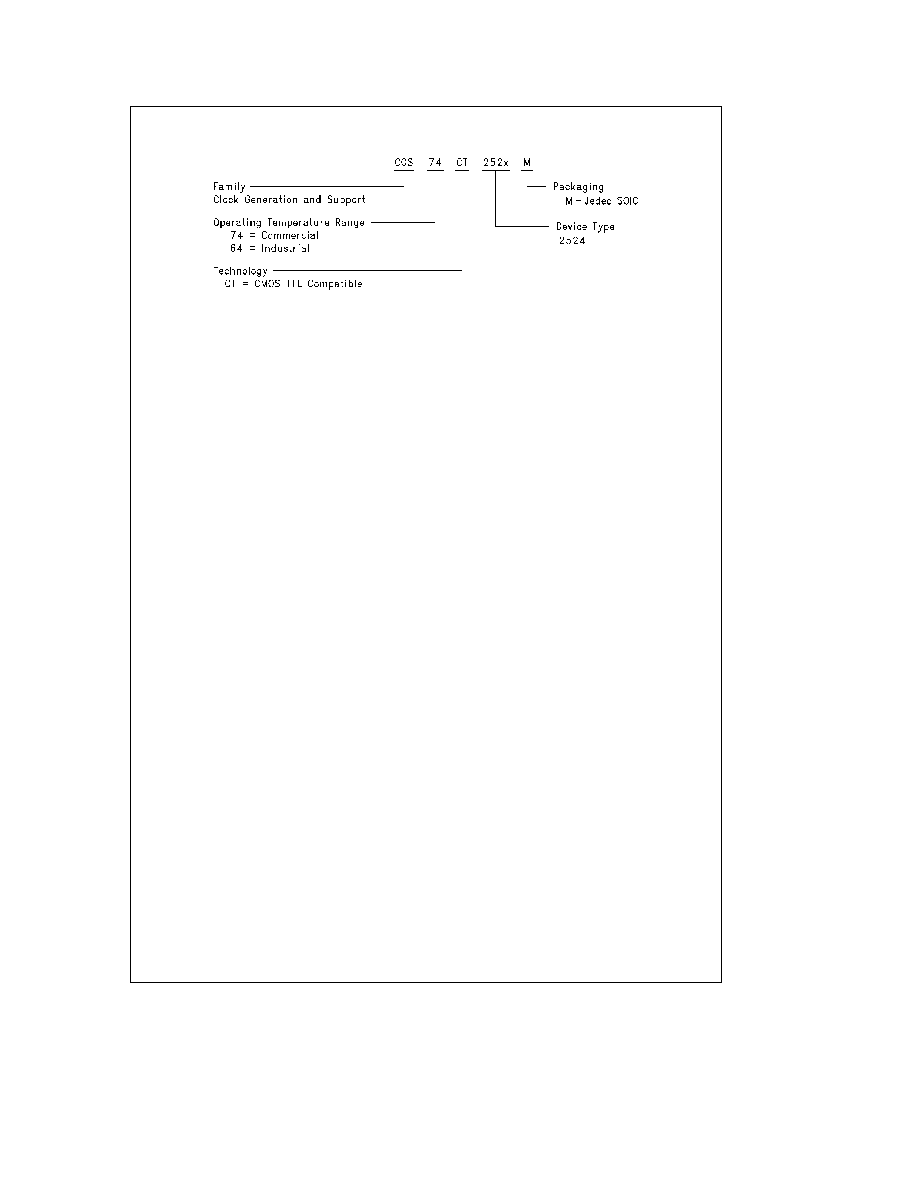
Ordering Information
Contact NSC Marketing for specific data of availability
TL F 11752 ≠ 14
5