CLC5526
Digital Variable Gain Amplifier (DVGA)
General Description
The CLC5526 is a high performance, digitally controlled,
variable-gain amplifier (DVGA). It has been designed for use
in a broad range of mixed signal and digital communication
applications such as mobile radio, cellular base stations and
back-channel modems where automatic-gain-control (AGC)
is required to increase system dynamic range.
The CLC5526 has differential input and output, allowing
large signal swings on a single 5V rail. The input impedance
is 200
. The differential output impedance is 600 and is
designed to drive a 1 k
differential load. The output ampli-
fier
has
excellent
intermodulation
performance.
The
CLC5526 is designed to accept signals from RF elements
and maintain a terminated impedance environment.
The CLC5526 maintains a 350 MHz bandwidth over its
entire gain and attenuation range from +30 dB to -12 dB.
Internal clamping ensures very fast overdrive recovery. Two
tone intermodulation distortion is excellent: at 150 MHz, 1
V
pp
it is -64 dBc.
Input signals to the CLC5526 are scaled by an accurate,
differential R-2R resistive ladder with an input impedance of
200
. A scaled version of the input is selected under digital
control and passed to the internal amplifier. The input com-
mon mode level is set at 2.4V via a bandgap referenced bias
generator which can be overridden by an external input.
Following the resistive ladder is a fixed, 30 dB gain amplifier.
The output stage common mode voltage of the CLC5526 is
set to 3V, by internal, positive supply connected resistors.
Digital control of the CLC5526 is accomplished by a 3-bit
parallel gain control input and a data valid pin to latch the
data. If the data is not latched, the DVGA is transparent to
gain control updates. All digital inputs are TTL/CMOS com-
patible.
A shutdown input reduces the CLC5526 supply currrent to a
few mA. During shutdown, the input termination is main-
tained and current attenuation settings are held.
The CLC5526 operates over the industrial temperature
range of -40∞C to +85∞C. The part is available in a 20-pin
SSOP package.
Features
n
350 MHz bandwidth
n
Differential input and output
n
Gain control: parallel w/data latching
n
Supply voltage:
+5V
n
Supply current:
48 mA
Key Specifications
n
Low two tone intermod:
distortion: -64 dBc
@
1 V
PP
, 150 MHz
24.5 dBm IP3, 150 MHz
n
Low noise:
2.5 nV/
Hz (max gain),
9.3 dB noise figure (max gain)
n
Wide gain range:
+30 dB to -12 dB
n
Gain step size:
6 dB
Applications
n
Cellular/PCS base stations
n
IF sampling receivers
n
Infrared/CCD imaging
n
Back-channel modems
n
Electro-optics
n
Instrumentation
n
Medical imaging
n
High definition video
September 2002
CLC5526
Digital
V
ariable
Gain
Amplifier
(DVGA)
© 2002 National Semiconductor Corporation
DS015016
www.national.com
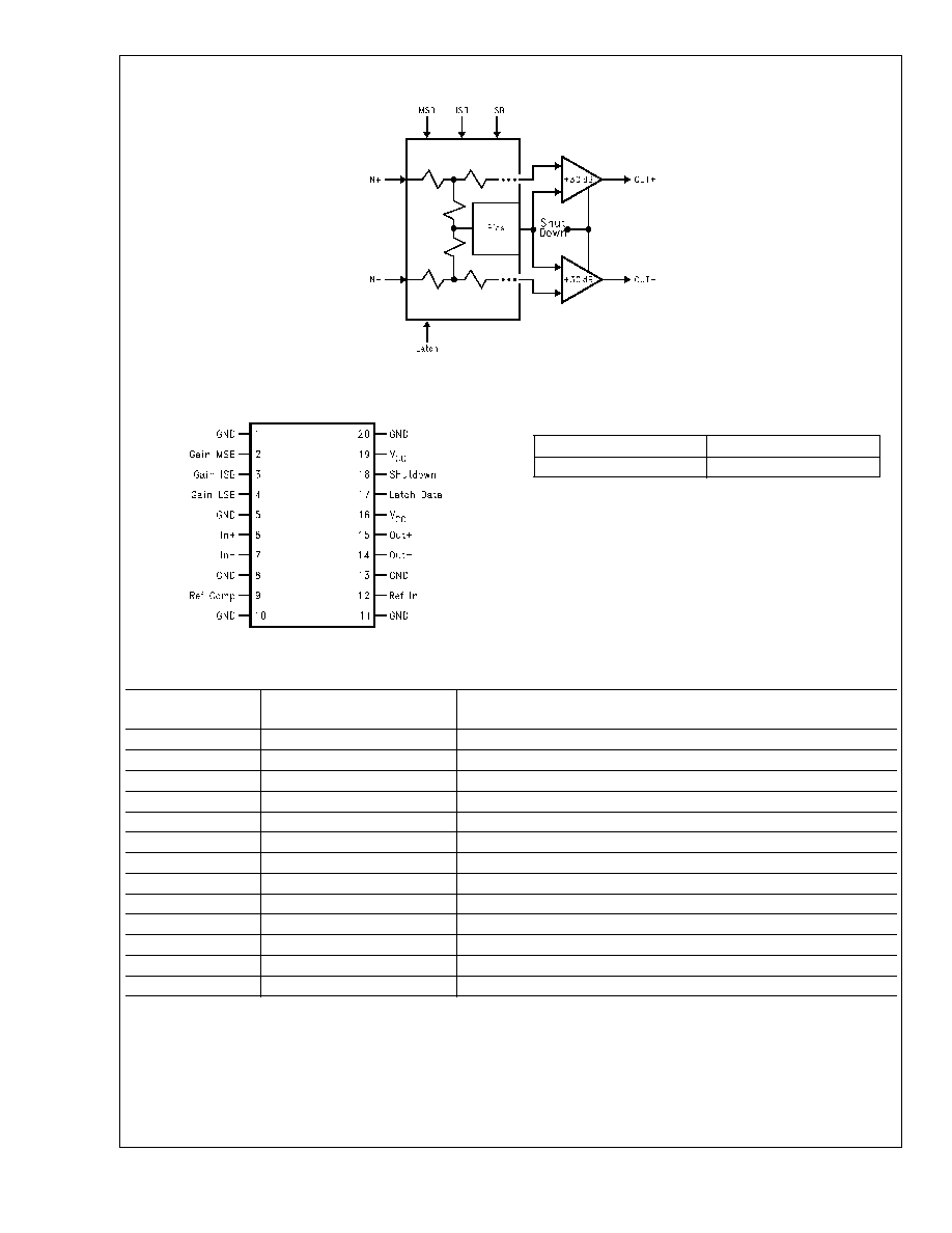
Block Diagram
01501602
Pin Configuration
01501601
Ordering Information
CLC5526MSA
20-Pin SSOP
CLC5526PCASM
Evaluation Board
Pin Descriptions
Pin
Name
Pin
No.
Description
GND
1, 5, 8, 10, 11, 13, 20
Circuit ground.
Gain MSB
2
Gain Selection Most Significant Bit
Gain ISB
3
Gain Selection Data Bit
Gain LSB
4
Gain Selection Least Significant Bit
In+
6
Positive Differential Input
In-
7
Negative Differential Input
Ref Comp
9
Reference Compensation
V
CC
16, 19
Positive Supply Voltage
Shutdown
18
Low Power Standby Control (Active High)
Latch Data
17
Data Latch Control (Active High)
Out+
15
Positive Differential Output
Out-
14
Negative Differential Output
Ref In
12
External Reference Input
CLC5526
www.national.com
2
Absolute Maximum Ratings
(Note 1)
If Military/Aerospace specified devices are required,
please contact the National Semiconductor Sales Office/
Distributors for availability and specifications.
Positive Supply Voltage (V
CC
)
-0.5V to +6V
Differential Voltage between any
Two Grounds
<
200 mV
Analog Input Voltage Range
-0.5V to +V
CC
Digital Input Voltage Range
-0.5V to +V
CC
Output Short Circuit Duration
(one-pin to ground)
Infinite
Junction Temperature
150∞C
Storage Temperature Range
-65∞C to +150∞C
Lead Solder Duration (+300∞C)
10 sec
Recommended Operating
Conditions
Positive Supply Voltage (V
CC
)
+5V
±
5%
Differential Voltage between any
Two Grounds
<
10 mV
Analog Input Voltage Range, AC
Coupled
±
0.5V
Operating Temperature Range
-40∞C to +85∞C
Package Thermal Resistance
Package
(
JA
)
(
JC
)
20-Pin SSOP
90∞C/W
38∞C/W
Reliability Information
Transistor Count
300
Electrical Characteristics
The following specifications apply for V
CC
= +5V, R
L
= 1 k
maximum gain setting. Boldface limits apply for T
A
= T
min
=
-40∞C to T
max
= +85∞C, all other limits T
A
= 25∞C (Notes 2, 3, 4).
Symbol
Parameter
Conditions
Min
Typ
Max
Units
DYNAMIC PERFORMANCE
BW
Small-Signal Bandwidth
350
MHz
NOISE AND DISTORTION
2nd Harmonic Distortion
f
IN
= 150 MHz, 1 V
PP
53
67
dBc
f
IN
= 250 MHz, 1 V
PP
64
dBc
f
IN
= 150 MHz, 2 V
PP
43
62
dBc
f
IN
= 250 MHz, 2 V
PP
58
dBc
3rd Harmonic Distortion
f
IN
= 150 MHz, 1 V
PP
53
71
dBc
f
IN
= 250 MHz, 1 V
PP
70
dBc
f
IN
= 150 MHz, 2 V
PP
43
57
dBc
f
IN
= 250 MHz, 2 V
PP
56
dBc
IMD
Two Tone Intermodulation
Distortion
f
1
= 149.9 MHz, f
2
= 150.1 MHz,
1 V
PP
Composite
64
dBc
f
1
= 149.9 MHz, f
2
= 150.1 MHz,
2 V
PP
Composite
61
dBc
f
1
= 249.9 MHz, f
2
= 250.1 MHz,
1 V
PP
Composite
63
dBc
f
1
= 249.9 MHz, f
2
= 250.1 MHz,
2 V
PP
Composite
54
dBc
Two Tone, 3rd Order
Intermodulation
150 MHz
24.5
dBm
Thermal Noise
Minimum Gain Setting
2.2
nV/
Hz
Maximum Gain Setting
2.5
nV/
Hz
Noise Figure
Maximum Gain Setting
9.3
dB
ANALOG I/O
Differential Input Impedance
200
Differential Output Impedance
600
Input Signal Level (AC Coupled)
Maximum Gain
126
mV
Maximum Input Signal Level
Recommended
6
V
PP
Maximum Output Signal Level
Recommended
4
V
PP
Output Clipping
8
V
PP
GAIN PARAMETERS
CLC5526
www.national.com
3
Electrical Characteristics
(Continued)
The following specifications apply for V
CC
= +5V, R
L
= 1 k
maximum gain setting. Boldface limits apply for T
A
= T
min
=
-40∞C to T
max
= +85∞C, all other limits T
A
= 25∞C (Notes 2, 3, 4).
Symbol
Parameter
Conditions
Min
Typ
Max
Units
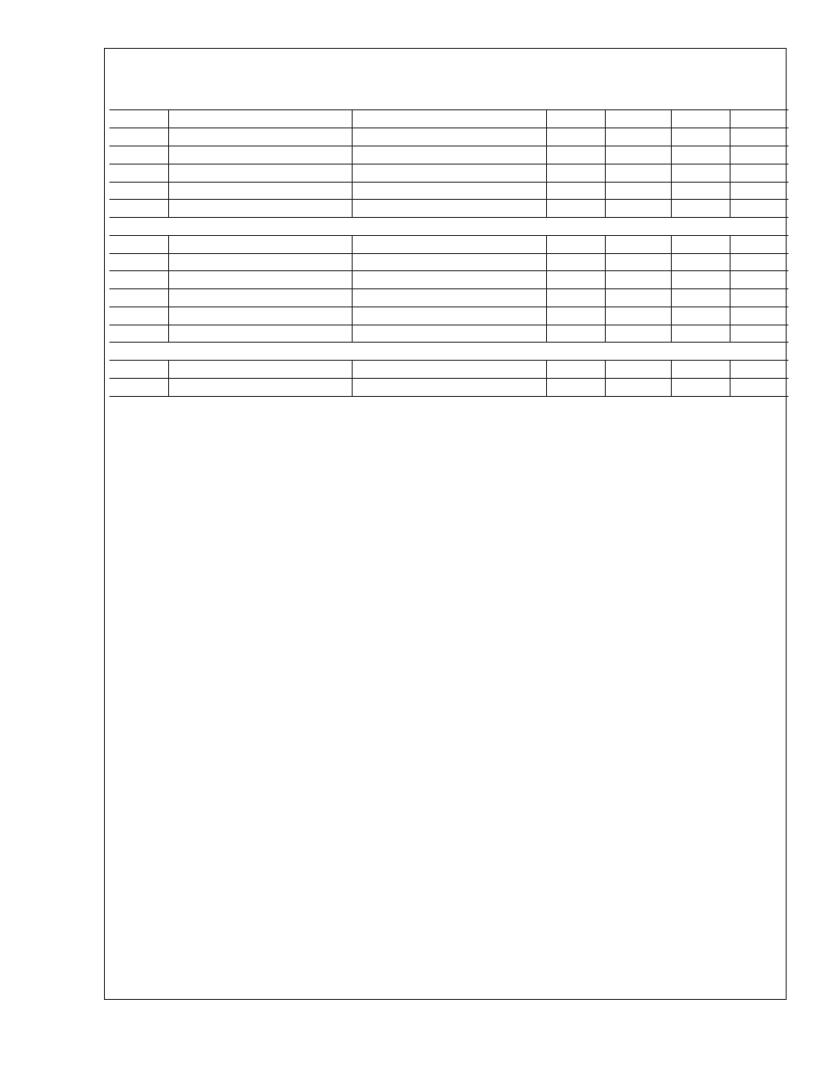
Maximum Gain
30
dB
Minimum Gain
-12
dB
Gain Step Size
6.02
dB
Gain Step Accuracy
(1 sigma)
0.03
dB
Cumulative Gain Step Error
(1 sigma)
0.085
dB
DIGITAL INPUTS/TIMING
Logic Compatibility
TTL/CMOS
V
V
IL
Logic Input Low Voltage
0.8
V
V
IH
Logic Input High Voltage
2.0
V
T
SU
Setup Time
3
ns
T
HOLD
Hold Time
3
ns
T
PW
Minimum Pulse Width
3
ns
POWER REQUIREMENTS
I
CC
+5V Supply Current
48
60
mA
Shutdown
9
mA
Note 1: "Absolute Maximum Ratings" are limited values, to be applied individually, and beyond which the serviceability of the circuit may be impaired. Functional
operability under any of these conditions is not necessarily implied. Exposure to maximum ratings for extended periods may affect device reliability.
Note 2: Limits are 100% tested at 25∞C.
Note 3: Typical specifications are the mean values of the distributions of deliverable amplifiers tested to date.
Note 4: Outgoing quality levels are determined from tested parameters.
CLC5526
www.national.com
4
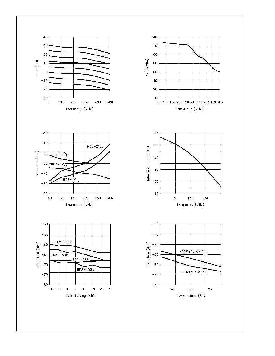
Typical Performance Characteristics
(V
CC
= +5V, R
L
= 1 k
, max gain; unless specified)
Gain vs. Frequency
Transconductance vs. Frequency
01501603
01501604
2nd and 3rd Harmonic Distortion
vs. Frequency
2-Tone, 3rd Order Intermodulation
Output Intercept vs Frequency
01501605
01501606
Distortion vs. Gain Setting
Distortion vs. Temperature
01501607
01501608
CLC5526
www.national.com
5