 | –≠–ª–µ–∫—Ç—Ä–æ–Ω–Ω—ã–π –∫–æ–º–ø–æ–Ω–µ–Ω—Ç: CLC5801IM | –°–∫–∞—á–∞—Ç—å:  PDF PDF  ZIP ZIP |
CLC5801
High Speed Low Noise Voltage Feedback Amplifier
General Description
The CLC5801 is a low-cost, wideband voltage feedback
amplifier excellent for low noise applications. It combines
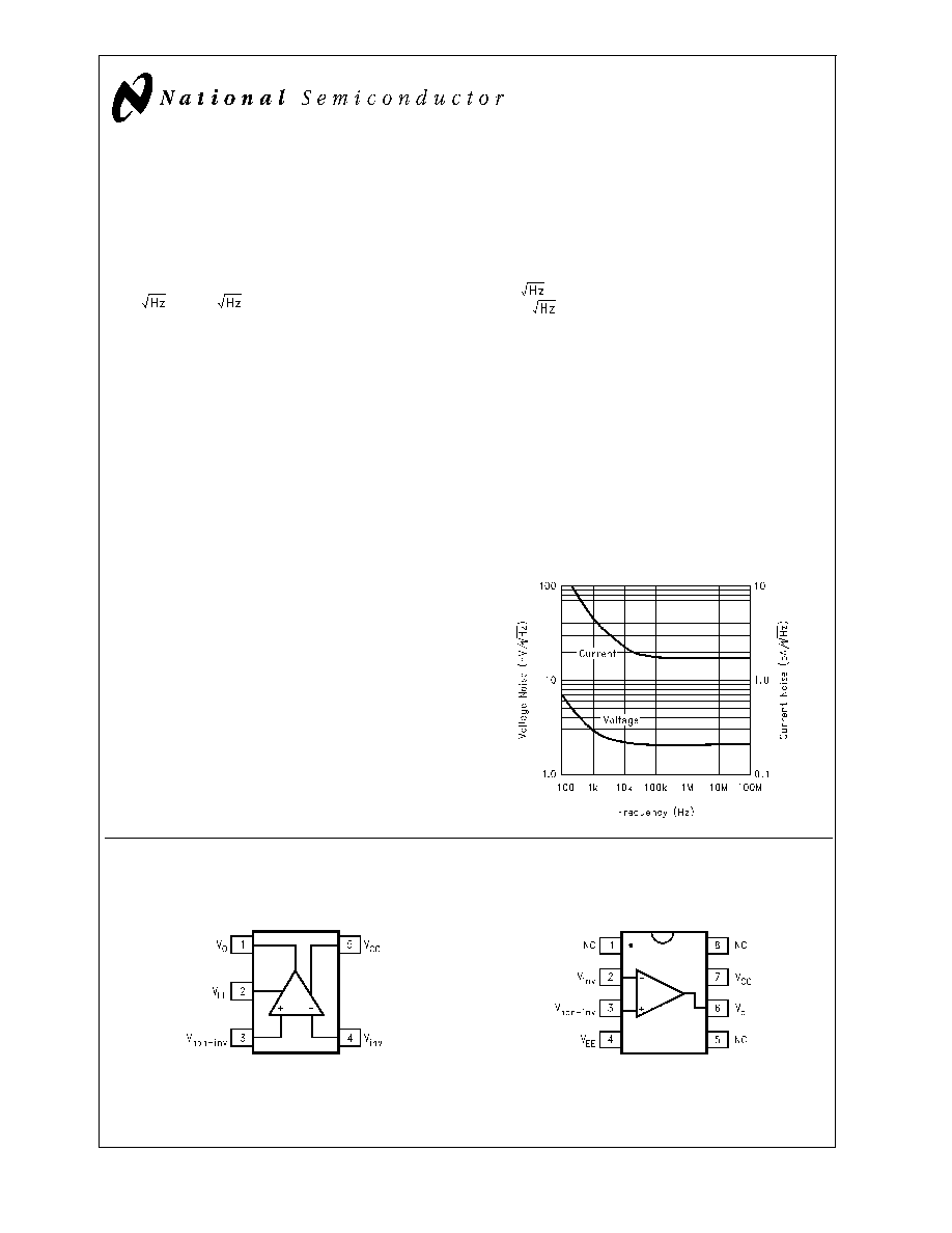
a wide bandwidth of 420MHz with very low noise
(2nV/
, 1.8pA/
) and low DC errors (100µV V
OS
)
making it an excellent precision high speed op amp offering
closed-loop gains of
10.
The CLC5801 employs a traditional voltage-feedback topol-
ogy and provides all the benefits of balanced inputs, such as
low offsets and drifts, as well as 96dB open-loop gain, 95dB
CMRR and a 90dB PSRR. Providing a wide 420MHz band-
width at a gain of A
V
= 10, a fast 300V/µs slew rate, the
CLC5801 is well suited for wide band active filters and low
noise loop filters for PLLs.
The low noise, wide gain-bandwidth, high slew rate and low
DC errors enable applications such as medical diagnostic ul-
trasound, magnetic tape and disk storage, communications
and optoelectronics that require maximum high-frequency
signal-to-noise ratios. Low noise and offset make the
CLC5801 and ideal preamplifier for CD-ROMs and receiv-
ers.
The CLC5801 consumes 16mA of supply current and can be
used in either dual 5V systems or single supply applications.
It can easily drive a 100
load to within 1.6V of either rail.
The CLC5801 is available in both SOIC-8 and the tiny
SOT23-5.
Features
(T
A
= 25∞C, V
S
=
±
5V, R
L
= 100
Typical unless specified).
n
420MHz, -3dB bandwidth (A
V
= 10)
n
2nV/
input voltage noise
n
1.8pA/
input current noise
n
100µV input offset voltage
n
300V/µs slew rate
n
16mA supply current
n
18ns settling time
Applications
n
Ultrasound preamplifier
n
CD-ROM preamplifer
n
Photo-diode transimpedance amplifier
n
Low-noise loop filters for PLLs
n
High-performance receivers
n
ADC preamplifier
Connection Diagrams
Equivalent Input Noise
DS101307-1
5-Pin SOT23-5
DS101307-2
Top View
8-Pin SOIC
DS101307-3
Top View
May 2000
CLC5801
High
Speed
Low
Noise
V
oltage
Feedback
Amplifier
© 2000 National Semiconductor Corporation
DS101307
www.national.com
Ordering Information
Package
Part Number
Packaging
Marking
Transport Media
NSC
Drawing
8-pin SOIC
CLC5801IM
CLC5801IM
Rails
M08A
CLC5801IMX
CLC5801IM
2.5k Tape and Reel
5-pin SOT23-5
CLC5801IM5
A50A
1k Units Tape and Reel
MF05A
CLC5801IM5X
A50A
3k Units Tape and Reel
CLC5801
www.national.com
2
Absolute Maximum Ratings
(Note 1)
If Military/Aerospace specified devices are required,
please contact the National Semiconductor Sales Office/
Distributors for availability and specifications.
V
CC
±
7V
I
OUT
Short Circuit protected to
ground. Maximum reliability is
obtained if I
OUT
does not exceed:
125mA
Common-Mode Input Voltage
±
V
CC
Maximum Junction Temperature
+125∞C
Storage Temperature Range
-65∞C to +150∞C
Lead Temperature (soldering 10 sec)
+300∞C
ESD (human body model)
1000V
Operating Rating
(Note 1)
Thermal Resistance (
JC
)
SOIC
65∞C/W
SOT23-5
115∞C/W
Thermal Resistance (
JA
)
SOIC
145∞C/W
SOT23-5
185∞C/W
Temperature Range
-40∞C to +85∞C
Recommended Gain Range
±
10 to
±
1000V/V
Electrical Characteristics
(T
A
= 25∞C, V
CC
=
±
5V, R
g
= 26.1
, R
f
= 499
, R
L
= 100
; unless specified).
Symbol
Parameter
Conditions
Typ
Min/Max Ratings
(Note 2)
Units
+25∞C
-40∞C
+25∞C
+85∞C
Frequency Domain Response
GBW
Gain Bandwidth Product
V
O
<
0.4V
PP
1.8
1.3
GHz
SSBW
-3dB Bandwidth (A
V
= +10)
V
O
<
0.4V
PP
420
MHz
-3dB Bandwidth (A
V
= +20)
V
O
<
0.4V
PP
90
70
LSBW
-3dB Bandwidth
V
O
<
5.0V
PP
35
30
GFP
Gain Flatness Peaking
DC to 30MHz, V
O
<
0.4V
PP
0.4
0.5
dB
GFR
Gain Flatness Rolloff
DC to 30MHz, V
O
<
0.4V
PP
0.2
0.5
dB
LPD
Linear Phase Deviation
DC to 30MHz, V
O
<
0.4V
PP
0.8
1.5
Deg
Time Domain Response
TRS
Rise and Fall Time
0.4V step
4.0
4.7
ns
TSS
Settling Time to 0.2%
2V step
18
30
ns
OS
Overshoot
0.4V step
5
10
%
SR
Slew Rate
2V step
300
250
V/µs
Distortion And Noise Response
HD2
2nd Harmonic Distortion
1V
PP
,10MHz
-53
-48
dBc
HD3
3rd Harmonic Distortion
1V
PP
,10MHz
-78
-65
dBc
IMD
3rd Order Intermod. Intercept
10MHz
34
dBm
VN
Equivalent Input Noise Voltage
1MHz to 100MHz
2.0
2.7
nV/
ICN
Equivalent Input Noise Current
1MHz to 100MHz
1.8
2.5
pA/
Static, DC Performance
AOL
Open-Loop Gain
DC
96
77
86
86
dB
VIO
Input Offset Voltage (Note 3)
±
100
±
1000
±
800
±
1000
µV
DVIO
Offset Voltage Average Drift
±
2
8
≠
4
µV/∞C
IB
Input Bias Current (Note 3)
12
40
20
20
µA
DIB
Bias Current Average Drift
-100
-250
≠
-120
µA/∞C
IIO
Input Offset Current
±
0.2
3.4
2.0
2.0
µA
DIIO
Offset Current Average Drift
±
3
±
50
≠
±
25
nA/∞C
PSRR
Power Supply Rejection Ratio
DC
90
80
85
84
dB
CMRR
Common Mode Rejection Ratio
DC
95
84
88
86
dB
ICC
Supply Current (Note 3)
R
L
=
16
18
17
17
mA
CLC5801
www.national.com
3
Electrical Characteristics
(Continued)
(T
A
= 25∞C, V
CC
=
±
5V, R
g
= 26.1
, R
f
= 499
, R
L
= 100
; unless specified).
Symbol
Parameter
Conditions
Typ
Min/Max Ratings
(Note 2)
Units
+25∞C
-40∞C
+25∞C
+85∞C
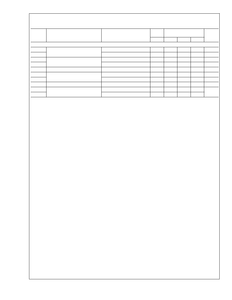
Miscellaneous Performance
RINC
Input Resistance
Common-Mode
2
0.6
1.6
1.6
M
RIND
Differential-Mode
6
1
3
3
k
CINC
Input Capacitance
Common-Mode
1.5
3
3
3
pF
CIND
Differential-Mode
1.9
3
3
3
pF
ROUT
Output Resistance
Closed Loop
5
50
10
10
m
VO
Output Voltage Range
R
L
=
±
3.8
±
3.5
±
3.7
±
3.7
V
VOL
R
L
= 100
±
3.4
±
2.8
±
3.2
±
3.2
V
CMIR
Input Voltage Range
Common-Mode
±
3.8
±
3.4
±
3.5
±
3.5
V
IOP
Output Current
Source
80
60
65
65
mA
ION
Sink
80
40
55
55
Note 1: "Absolute Maximum Ratings" are those values beyond which the safety of the device cannot be guaranteed. They are not meant to imply that the devices
should be operated at these limits. The table of "Electrical Characteristics" specifies conditions of device operation. Operating Ratings indicate conditions for which
the device is intended to be functional, but specific performance is not guaranteed,
Note 2: Min/max ratings are based on product characterization and simulation. Individual parameters are tested as noted. Outgoing quality levels are determined
from tested parameters.
Note 3: 100% tested at +25∞C.
CLC5801
www.national.com
4
Typical Performance Characteristics
(T
A
= 25∞C, V
CC
=
±
5V, R
g
= 26.1
, R
f
= 499
, R
L
= 100
,
unless otherwise specified).
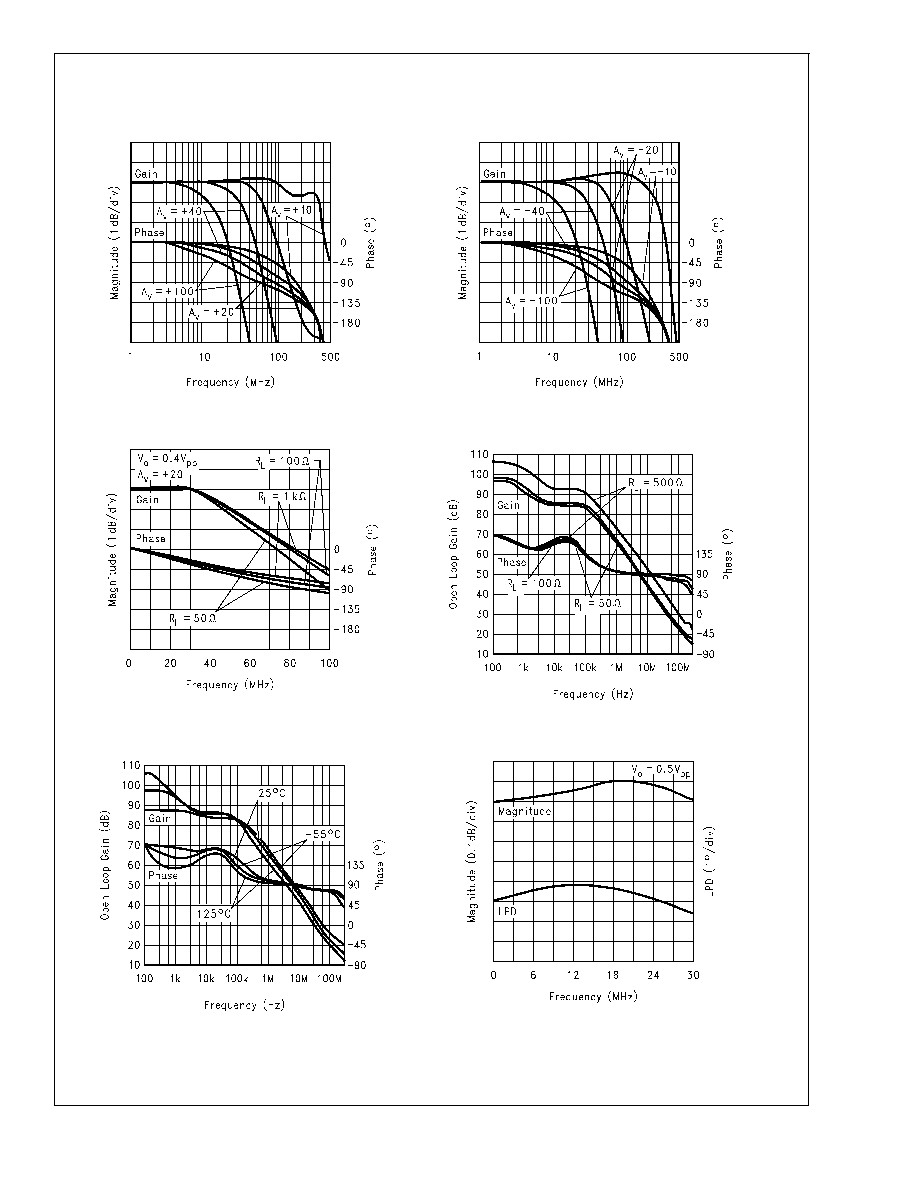
Non-Inverting Frequency Response
DS101307-4
Inverting Frequency Response
DS101307-5
Frequency Response for Various R
L
s
DS101307-6
Open Loop Gain and Phase vs. R
L
DS101307-7
Open Loop Gain and Phase vs. Temp
DS101307-8
Gain Flatness & Linear Phase Deviation
DS101307-9
CLC5801
www.national.com
5