CLC5802
Dual Low-Noise, Voltage Feedback Op Amp
General Description
The CLC5802 is a dual op amp that offers a traditional
voltage-feedback topology featuring unity-gain stability. Low
noise and very low harmonic distortion combine to form a
very wide dynamic-range op amp that operates within a
power supply range of 5V to 12V.
Each of the CLC5802's closely matched channels provides a
140MHz unity-gain bandwidth with a very low input voltage
noise density (4nV/
). Low 2nd/3rd harmonic distortion
(-69/-66dBc) as well as high channel-to-channel isolation
(-61dB) make the CLC5802 a perfect wide dynamic-range
amplifier for I/Q channels and other application which require
low distortion and matching. With its fast and accurate set-
tling (18ns to 0.1%), the CLC5802 is also a excellent choice
for wide-dynamic range, anti-aliasing filters to buffer the in-
puts of hi-resolution analog-to-digital converters. Combining
the CLC5802 two tightly-matched amplifiers in a single
eight-pin SOIC reduces cost and board space for many com-
posite amplifier applications such as active filters, differential
line drivers/receivers, fast peak detectors and instrumenta-
tion amplifiers.
Features
(T
A
= 25∞C, V
S
=
±
5V, R
L
= 100
, Typical unless specified).
n
Wide unity-gain bandwidth: 140MHz
n
Ultra-low noise: 4nV/
, 2pA/
n
Low distortion: -69/-66dBc (5MHz)
n
Settling time: 18ns to 0.1%
n
High output current:
±
70mA
n
Supply voltage range: 5V to 12V
Applications
n
General purpose dual op amp
n
Low noise active filters
n
Low noise integrators
n
High-speed detectors
n
Diff-in/diff-out instrumentation amp
n
I/Q channel amplifiers
n
Driver/receiver for transmission systems
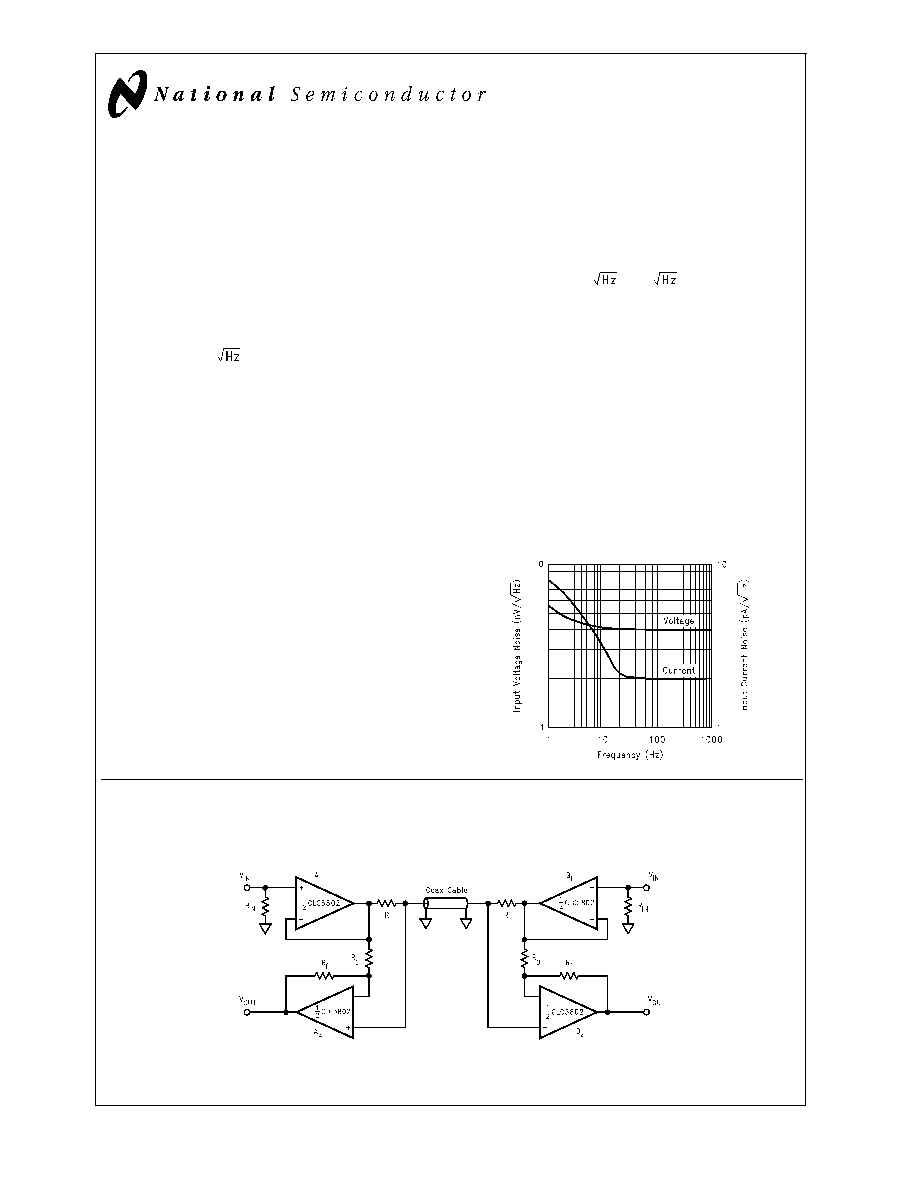
Typical Application
Equivalent Input Noise
DS101341-16
Full Duplex Transmission
DS101341-28
May 2000
CLC5802
Dual
Low-Noise,
V
oltage
Feedback
Op
Amp
© 2000 National Semiconductor Corporation
DS101341
www.national.com
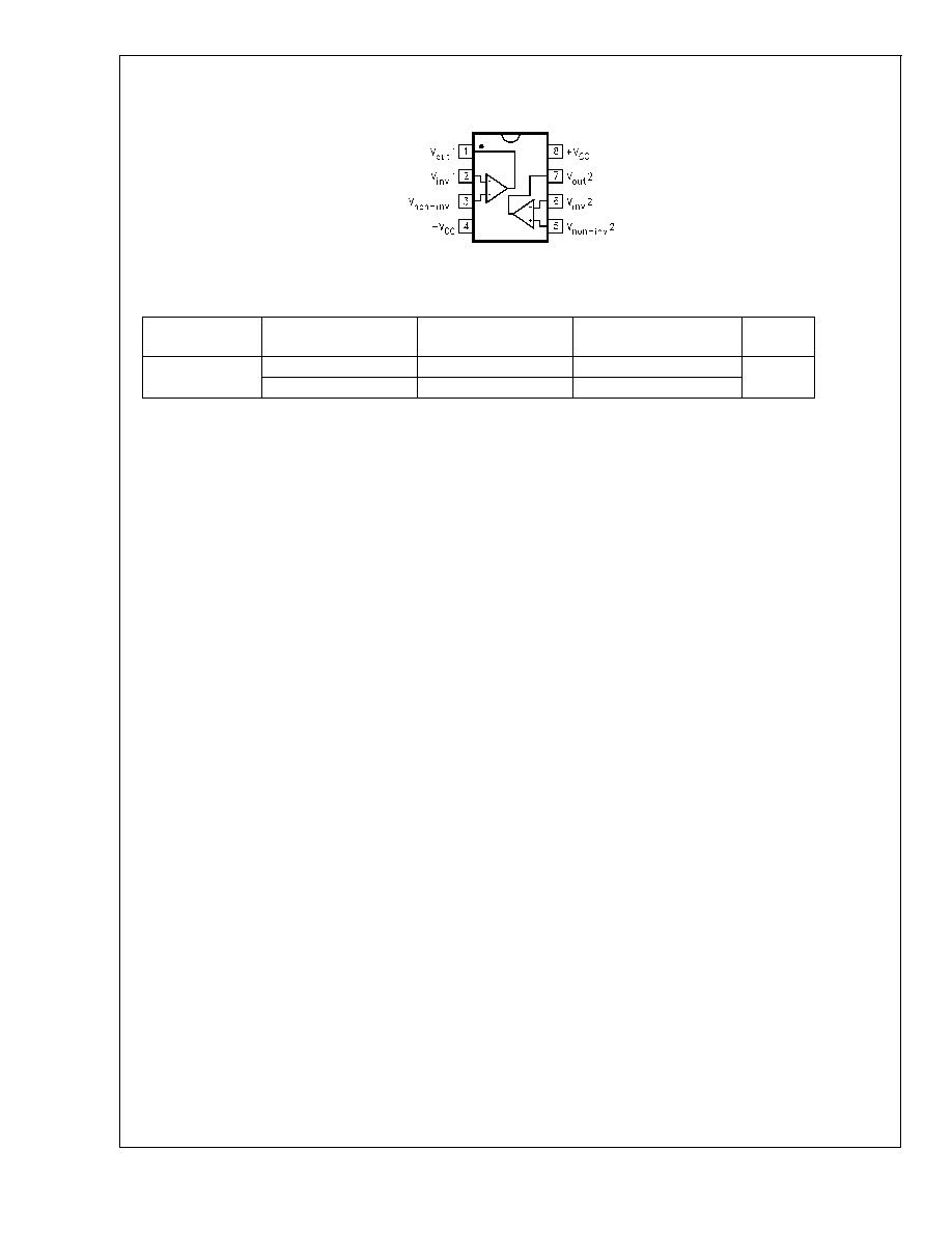
Connection Diagram
Ordering Information
Package
Part Number
Packaging
Marking
Transport Media
NSC
Drawing
8-pin SOIC
CLC5802IM
CLC5802IM
Rails
M08A
CLC5802IMX
CLC5802IM
2.5k Tape and Reel
8-Pin SOIC
DS101341-2
Top View
CLC5802
www.national.com
2
Absolute Maximum Ratings
(Note 1)
If Military/Aerospace specified devices are required,
please contact the National Semiconductor Sales Office/
Distributors for availability and specifications.
Supply Voltage
±
7V
Short Circuit Current
(Note 3)
Common-Mode Input Voltage
±
V
CC
Differential Input Voltage
±
10V
Maximum Junction Temperature
+125∞C
Storage Temperature
-65∞C to +150∞C
Lead Temperature (soldering 10 sec)
+300∞C
Operating Rating
(Note 1)
Thermal Resistance (
JC
)
40∞C/W
Thermal Resistance (
JA
)
115∞C/W
Temperature Range
-40∞C to +85∞C
Supply Voltage Range
5V to 12V
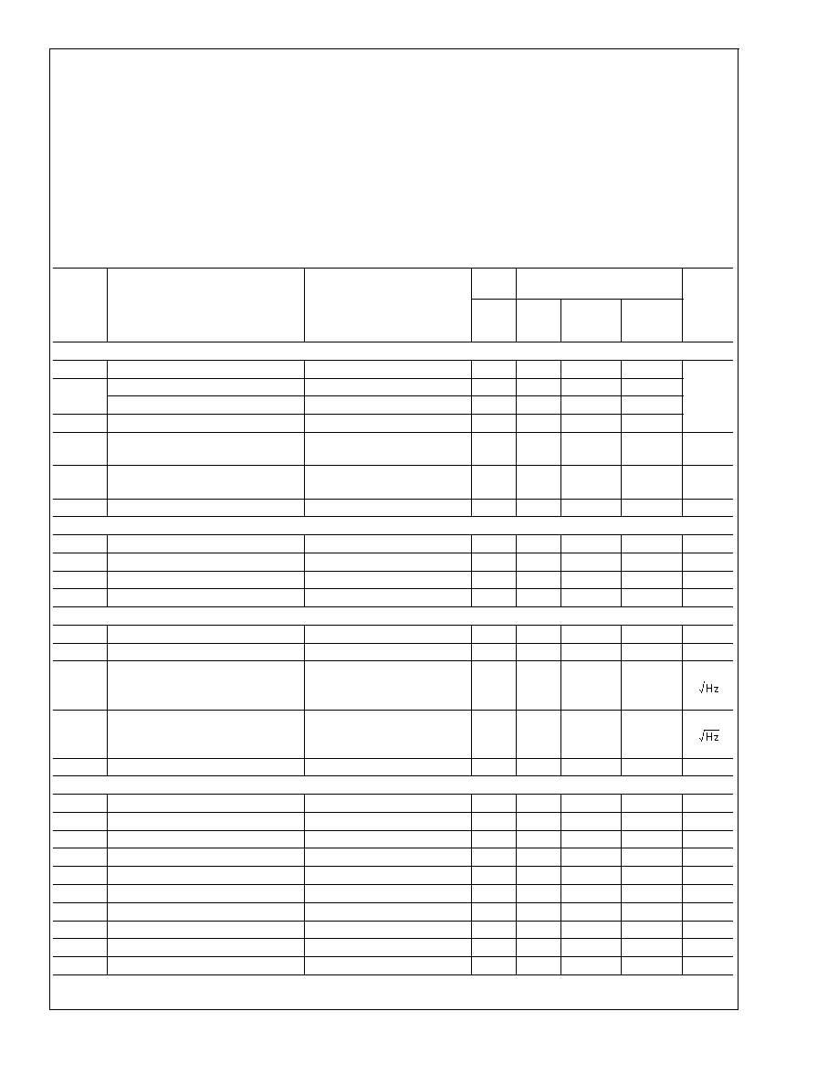
Electrical Characteristics
(T
A
= +25∞C, V
CC
=
±
5V, A
V
= +2V/V, R
f
= 100
, R
g
= 100
, R
L
= 100
; unless specified).
Symbol
Parameter
Conditions
Typ
Min/Max Ratings
(Note 2)
Units
+25∞C
+25∞C
0∞C to
+70∞C
-40∞C
to
+85∞C
Frequency Domain Response
GBW
Gain Bandwidth Product
V
OUT
<
0.5V
PP
120
90
MHz
SSBW
-3dB Bandwidth (A
V
= +1)
V
OUT
<
0.5V
PP
140
110
-3dB Bandwidth (A
V
= +2)
V
OUT
<
0.5V
PP
75
50
LSBW
-3dB Bandwidth
V
OUT
<
5.0V
PP
40
25
GFP
Gain Flatness Peaking
DC to 200MHz, V
OUT
<
0.5
V
PP
0.0
0.6
dB
GFR
Gain Flatness Rolloff
DC to 20MHz, V
OUT
<
0.5
V
PP
0.05
0.5
dB
LPD
Linear Phase Deviation
DC to 20MHz
0.2
1.0
Deg
Time Domain Response
TRS
Rise and Fall Time
1V step
6
8
ns
TSS
Settling Time
2V step to 0.1%
18
22
ns
OS
Overshoot
1V step
1
5
%
SR
Slew Rate
5V step
450
275
V/µs
Distortion And Noise Response
HD2
2nd Harmonic Distortion
1V
PP
, 5MHz
-69
-57
dBc
HD3
3rd Harmonic Distortion
1V
PP
, 5MHz
-66
-54
dBc
VN
Equivalent Input Noise Voltage
1MHz to 100MHz
4.0
4.5
nV/
ICN
Equivalent Input Noise Current
1MHz to 100MHz
2.0
3.0
pA/
CT
Crosstalk
Input referred, 10MHz
-61
-58
dB
Static, DC Performance
AOL
Open-Loop Gain
DC
60
56
50
50
dB
VIO
Input Offset Voltage (Note 4)
±
1.0
±
2.0
±
3.0
±
3.5
mV
DVIO
Offset Voltage Average Drift
5
≠
15
20
µV/∞C
IB
Input Bias Current (Note 4)
1.5
25
40
65
µA
DIB
Bias Current Average Drift
150
≠
600
700
nA/∞C
IIO
Input Offset Current
0.3
3
5
5
µA
DIIO
Offset Current Average Drift
5
≠
25
50
nA/∞C
PSRR
Power Supply Rejection Ratio
DC
63
57
55
55
dB
CMRR
Common Mode Rejection Ratio
DC
60
54
52
52
dB
ICC
Supply Current (Note 4)
Per Channel, R
L
=
11
12
13
15
mA
CLC5802
www.national.com
3
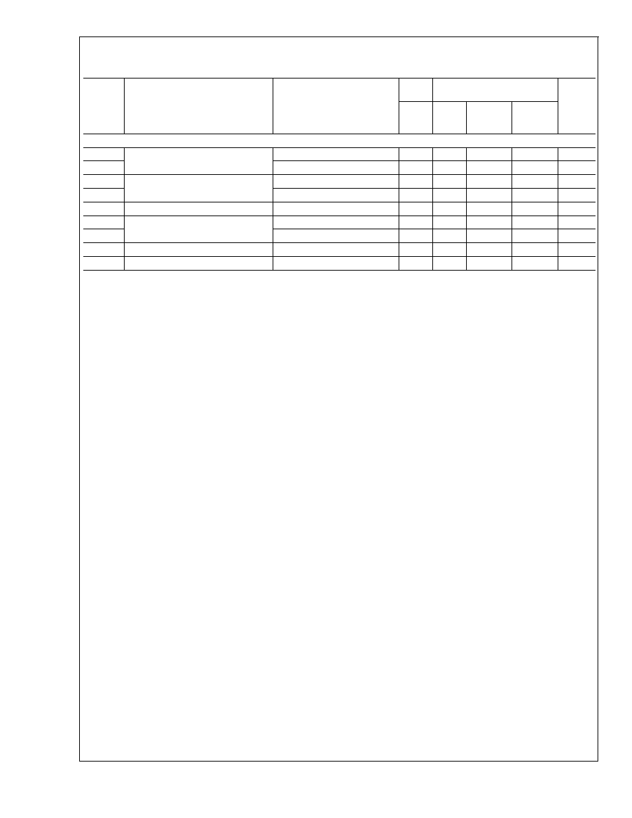
Electrical Characteristics
(Continued)
(T
A
= +25∞C, V
CC
=
±
5V, A
V
= +2V/V, R
f
= 100
, R
g
= 100
, R
L
= 100
; unless specified).
Symbol
Parameter
Conditions
Typ
Min/Max Ratings
(Note 2)
Units
+25∞C
+25∞C
0∞C to
+70∞C
-40∞C
to
+85∞C
Miscellaneous Performance
RINC
Input Resistance
Common-Mode
500
250
125
125
k
RIND
Differential-Mode
200
50
25
25
k
CINC
Input Capacitance
Common-Mode
2.0
3.0
3.0
3.0
pF
CIND
Differential-Mode
2.0
3.0
3.0
3.0
pF
ROUT
Output Resistance
Closed Loop
0.05
0.1
0.2
0.2
VO
Output Voltage Range
R
L
=
±
3.6
±
3.5
±
3.3
±
3.3
V
VOL
R
L
= 100
±
3.4
±
3.2
±
2.6
±
1.3
V
CMIR
Input Voltage Range
Common-Mode
±
3.7
±
3.5
±
3.3
±
3.3
V
IO
Output Current
±
70
±
50
±
40
±
20
mA
Note 1: "Absolute Maximum Ratings" are those values beyond which the safety of the device cannot be guaranteed. They are not meant to imply that the devices
should be operated at these limits. The table of "Electrical Characteristics" specifies conditions of device operation. Operating Ratings indicate conditions for which
the device is intended to be functional, but specific performance is not guaranteed,
Note 2: Min/max ratings are based on product characterization and simulation. Individual parameters are tested as noted. Outgoing quality levels are determined
from tested parameters.
Note 3: Output is short circuit protected to ground, however maximum reliability is obtained if output current does not exceed 160mA.
Note 4: 100% tested at +25∞C.
CLC5802
www.national.com
4
Typical Performance Characteristics
(T
A
= 25∞C, V
CC
=
±
5V, R
g
= 26.1
, R
f
= 499
, R
L
= 100
,
unless otherwise specified).
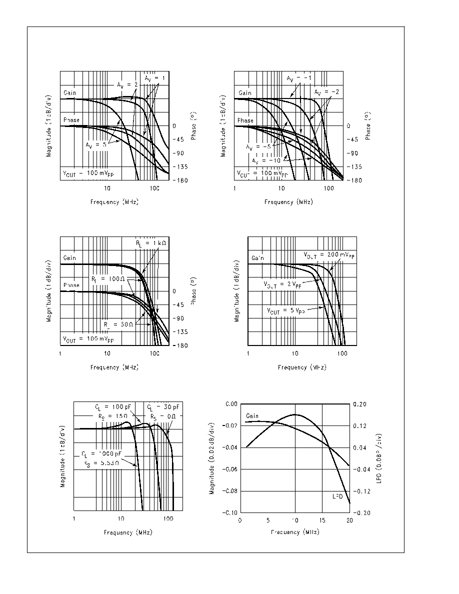
Non-Inverting Frequency Response
DS101341-3
Inverting Frequency Response
DS101341-4
Frequency Response vs. Load Resistance
DS101341-5
Frequency Response vs. Output Amplitude
DS101341-6
Frequency Response vs. Capacitive Load
DS101341-7
Gain Flatness & Linear Phase Deviation
DS101341-8
CLC5802
www.national.com
5