The CLC730075 and CLC730074 evaluation boards
are designed to aid in the characterization of National
Semiconductor's 14-pin, triple monolithic amplifiers.
s
CLC730075 - DIP packages
Uses all through-hole components
s
CLC730074 - SOIC packages
Uses all surface-mount components
Both boards have identical circuit configurations and are
designed for non-inverting gains. Inverting gains
or other circuit configurations can be obtained with slight
modifications to the boards. Use the evaluation boards
as a:
s
Guide for high frequency layout
s
Tool to aid in device testing and characterization
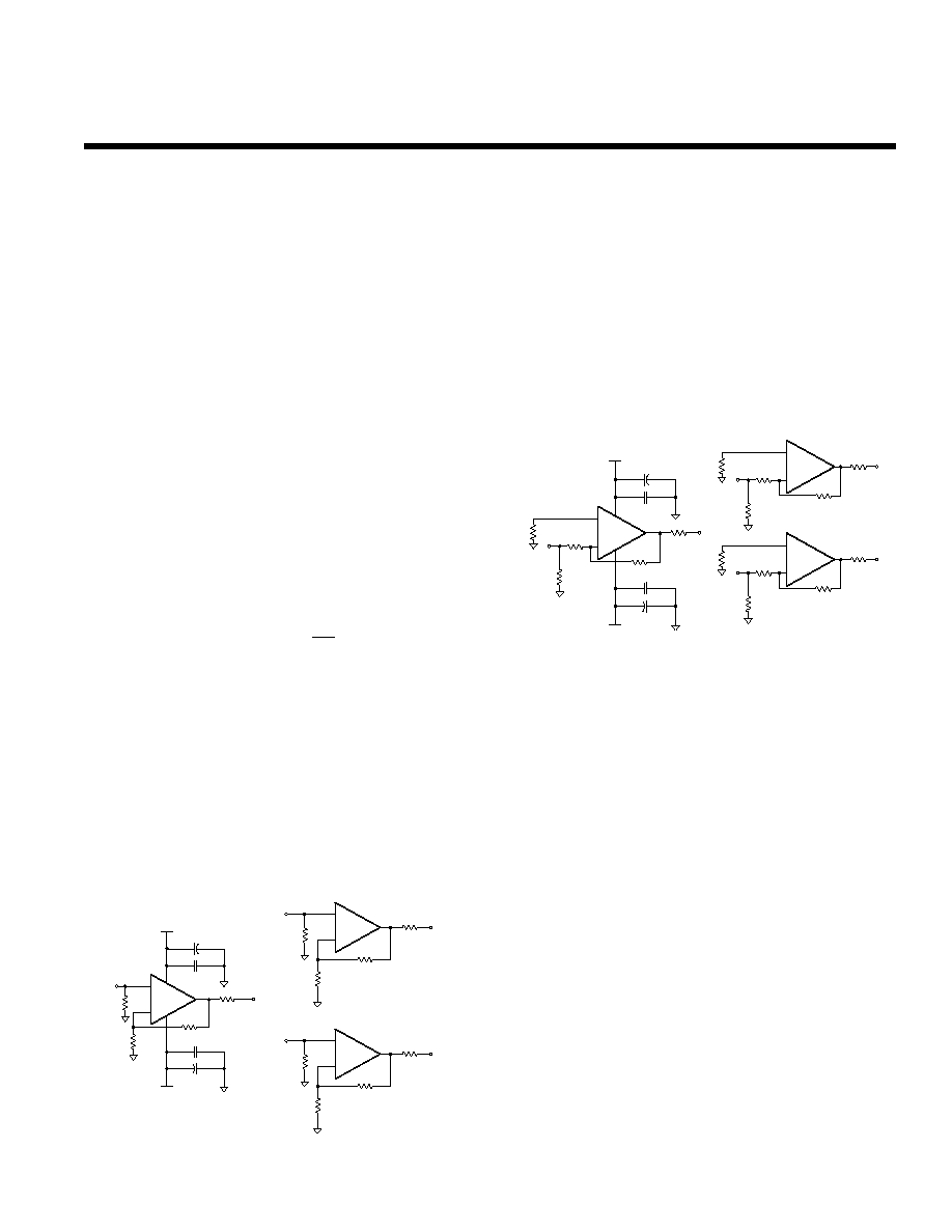
Basic Operation
Figure 1 shows the non-inverting schematic for both
boards. The input signal is brought into the board
through SMA connectors to the non-inverting input
of the amplifier. The resistor R
in
is used to set the
input termination resistance to the op amp. The non-
inverting gain is set by the following equation:
Non-inverting Gain:
The value of the feedback resistor, R
f
, has a strong
influence on AC performance. Refer to the product data
sheet for feedback resistor selection. The output of the
op amp travels through a series resistance, R
out
, and
then leaves the board through an SMA connector. The
series resistance, R
out
, matches transmission lines or
isolates the output from capacitive loads. The 0.1
�
F
capacitor, C5, is placed between the power pins of the
amplifier to improve harmonic distortion performance. If
C5 is placed directly across pins 4 and 11, refer to the
CLC730074 board, then the capacitor provides the best
improvement in distortion performance.
Figure 1: Non-inverting Gain Configurations
Inverting Gain Operation
The evaluation boards can be modified to provide an
inverting gain configuration. Complete these steps to
modify the board:
1. Cut the input trace
2. Use 25
for R
in
3. Terminate R
g
at the input trace instead of
ground
4. Add R
t
for desired input impedance (input
impedance = R
g
||R
t
)
Figure 2 illustrates the inverting schematic for both
boards.
Figure 2: Inverting Gain Configurations
Isolation and Channel Matching Performance
For maximum isolation between channels, proper power
supply decoupling is required. Always include the
bypass capacitors C1, C2, C3, and C4. The use of good
quality capacitors also helps to achieve better isolation
performance.
The evaluation boards have also been designed to mini-
mize channel-to-channel crosstalk. The input and output
pins of the amplifier are sensitive to the coupling of par-
asitic capacitances caused by power or ground planes
and traces. To reduce the influence of these parasitics,
the ground plane has been removed around these sen-
sitive nodes. In multilayer boards, remove both the
ground and power traces and planes around the input
and output pins.
Layout Considerations
General layout and supply bypassing play major roles in
high frequency performance. When designing your own
board, use the evaluation board as a guide and follow
these steps as a basis for high frequency layout:
1. Use a ground plane.
2. Include 6.8
�
F tantalum and 0.1
�
F ceramic
capacitors on both supplies.
14-Pin Triple Op Amp Eval. Boards
Part Numbers CLC730075, CLC730074
September 1997
+
-
Channel 1
R
f1
C
1
C
3
OUT
1
IN
1
+V
CC
C
2
C
4
-V
CC
5
6
11
4
7
+
+
R
g1
R
in1
R
out1
+
-
Channel 2
R
f2
R
g2
R
in2
12
13
14
R
out2
OUT
2
IN
2
+
-
Channel 3
R
f3
R
g3
R
in3
10
9
8
R
out3
OUT
3
IN
3
+
-
Channel 1
R
f1
C
1
C
3
OUT
1
IN
1
+V
CC
C
2
C
4
-V
CC
5
6
11
4
7
+
+
R
t1
25
R
in1
R
out1
R
g1
Select R
t
to yield desired
input impedance = R
g
||R
t
R
g2
+
-
Channel 2
R
f2
OUT
2
IN
2
12
13
14
R
t2
25
R
in2
R
out2
R
g3
+
-
Channel 3
R
f3
OUT
3
IN
3
10
9
8
R
t3
25
R
in3
R
out3
1
R
R
f
g
+
� 1997 National Semiconductor Corporation
http://www.national.com
Printed in the U.S.A.
N
3. Place the 6.8
�
F capacitors within 0.75 inches
of the power pins.
4. Place the 0.1
�
F capacitors less than 0.1
inches from the power pins.
5. Remove the ground plane under and around
the part, especially near the input and output
pins to reduce parasitic capacitance.
6. Minimize all trace lengths to reduce series
inductances.
7. Use individual flush-mount sockets, for prototyping.
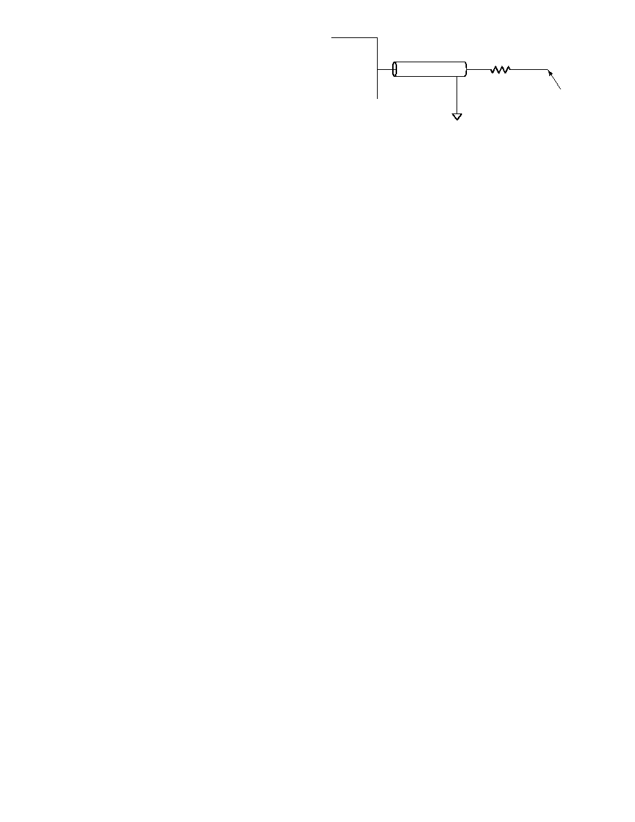
Measurement Hints
If 50
coax and 50
R
in
/R
out
resistors are used, many of
the typical performance plots found in the product data
sheets can be reproduced.
When SMA connectors and cables are not available to
evaluate the amplifier, do not use normal oscilloscope
probes. Use low impedance resistive divider probes of
100 to 500
. If a low impedance probe is not available,
then a section of 50
coaxial cable and a low impedance
resistor (10
to 50
) may be used. Follow these 3 steps
to create a "cable/resistor" probe:
1. Connect one end of the coax's center to a test
measurement box terminated in 50
.
2. Connect the other end of the cable's center
conductor to the low impedance resistor. (The
open side of the resistor is now a probe.)
3. Connect the ground shield of the cable to
evaluation board ground and test box ground.
Figure 3: "Cable/Resistor" Probe Configuration
This "cable/resistor" probe, shown in Figure 3, forms a
voltage attenuator between the resistor and the 50
termination resistance of the test box. This method
allows measurements to be performed directly on the
output pin of the amplifier.
When evaluating only one channel on the board,
complete the following on the unused channel:
1. Included R
f
and R
g
as shown in Figure 1
2. Ground the input
3. Load the output with 50
to ground
Power Supplies
Refer to the product data sheet for the recommended
supply voltages.
Component Values
s
R
f
, R
g
- Use the product data sheet to
select values
s
R
in
, R
out
- 50
(Refer to
Basic Operation
section for details)
s
R
t
- Optional resistor for inverting gain
configurations (Refer
Inverting Gain
Operation section for details)
s
C3, C4 - 6.8
�
F tantalum capacitors
s
C1, C2, C5 - 0.1
�
F ceramic capacitors
http://www.national.com
2
Test Box and
Evaluation Board
Ground
50
Coaxial
Cable
Low Impedance
Resistor
Probe
Test Box
(terminated
in 50
)
3
http://www.national.com
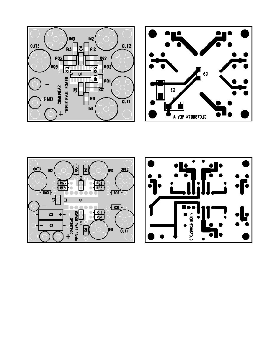
DIP � Top Side
DIP � Bottom Side
SOIC � Top Side
SOIC � Bottom Side

http://www.national.com
4
Lit #660904-001
Customer Design Applications Support
National Semiconductor is committed to design excellence. For sales, literature and technical support, call the
National Semiconductor Customer Response Group at 1-800-272-9959 or fax 1-800-737-7018.
Life Support Policy
National's products are not authorized for use as critical components in life support devices or systems without the express written approval of the
president of National Semiconductor Corporation. As used herein:
1. Life support devices or systems are devices or systems which, a) are intended for surgical implant into the body, or b) support or
sustain life, and whose failure to perform, when properly used in accordance with instructions for use provided in the labeling, can
be reasonably expected to result in a significant injury to the user.
2. A critical component is any component of a life support device or system whose failure to perform can be reasonably expected to
cause the failure of the life support device or system, or to affect its safety or effectiveness.
National Semiconductor
National Semiconductor
National Semiconductor
National Semiconductor
Corporation
Europe
Hong Kong Ltd.
Japan Ltd.
1111 West Bardin Road
Fax: (+49) 0-180-530 85 86
13th Floor, Straight Block
Tel: 81-043-299-2309
Arlington, TX 76017
E-mail: europe.support.nsc.com
Ocean Centre, 5 Canton Road
Fax: 81-043-299-2408
Tel: 1(800) 272-9959
Deutsch Tel: (+49) 0-180-530 85 85
Tsimshatsui, Kowloon
Fax: 1(800) 737-7018
English Tel: (+49) 0-180-532 78 32
Hong Kong
Francais Tel: (+49) 0-180-532 93 58
Tel: (852) 2737-1600
Italiano Tel: (+49) 0-180-534 16 80
Fax: (852) 2736-9960
National does not assume any responsibility for use of any circuitry described, no circuit patent licenses are implied and National reserves the right at any time without notice to change said
circuitry and specifications.
N