COP820C/840C Family
8-Bit CMOS ROM Based Microcontrollers with 1k or 2k
Memory
General Description
Note: COP8SA devices are instruction set and pinout com-
patible supersets of the COP800C Family devices, and are
replacements for these in new designs when possible.
The COP820C/840C Family ROM based microcontrollers
are integrated COP8
TM
Base core devices with smaller
memory (1k/2k), and fewer on-board features. These single-
chip CMOS devices are suited for lower-functionality appli-
cations where system cost is of prime consideration. Pin and
software compatible (different V
CC
range) 4k/32k OTP ver-
sions are available (COP87LxxCJ/RJ Family). Erasable win-
dowed versions are available for use with a range of COP8
software and hardware development tools.
Family features include an 8-bit memory mapped architec-
ture, 10 Hz CKI with 1µs instruction cycle, one multi-function
16-bit timer/counter with PWM, MICROWIRE/PLUS
TM
serial
I/O, power saving HALT mode, three clock modes, high cur-
rent outputs, software selectable I/O options, 2.3v-6.0v op-
eration and 20/28 pin packages.
Devices included in this datasheet are:
Device
Memory (bytes)
RAM
(bytes)
I/O Pins
Packages
Temperature
Comments
COP620C
1k ROM
64
24
28 DIP/SOIC
-55 to +125∞C
4.5v - 5.5v
COP820C
1k ROM
64
24
28 DIP/SOIC
-40 to +85∞C
COP920C
1k ROM
64
24
28 DIP/SOIC
0 to +70∞C
2.3v-4.0v,
CH=4.0v-6.0v
COP622C
1k ROM
64
16
20 DIP/SOIC
-55 to +125∞C
4.5v - 5.5v
COP822C
1k ROM
64
16
20 DIP/SOIC
-40 to +85∞C
COP922C
1k ROM
64
16
20 DIP/SOIC
0 to +70∞C
2.3v-4.0v,
CH=4.0v-6.0v
COP640C
2k ROM
128
24
28 DIP/SOIC
-55 to +125∞C
4.5v - 5.5v
COP840C
2k ROM
128
24
28 DIP/SOIC
-40 to +85∞C
COP940C
2k ROM
128
24
28 DIP/SOIC
0 to +70∞C
2.3v-4.0v,
CH=4.0v-6.0v
COP642C
2k ROM
128
16
20 DIP/SOIC
-55 to +125∞C
4.5v - 5.5v
COP842C
2k ROM
128
16
20 DIP/SOIC
-40 to +85∞C
COP942C
2k ROM
128
16
20 DIP/SOIC
0 to +70∞C
2.3v-4.0v,
CH=4.0v-6.0v
Key Features
n
16-bit multi-function timer supporting
-- PWM mode
-- External event counter mode
-- Input capture mode
n
1024 bytes ROM/64 bytes RAM-COP820C
n
2048 bytes ROM/128 bytes RAM-COP840C
I/O Features
n
Memory mapped I/O
n
Software selectable I/O options (TRI-STATE
Æ
Output,
Push-Pull Output, Weak Pull-Up Input, High Impedance
Input)
n
High current outputs
n
Schmitt trigger inputs on Port G
n
MICROWIRE/PLUS serial I/O
n
Packages:
-- 20 DIP/SO with 16 I/O pins
-- 28 DIP/SO with 24 I/O pins
CPU/Instruction Set Feature
n
1 µs instruction cycle time
n
Three multi-source interrupts servicing
-- External interrupt with selectable edge
-- Timer interrupt
-- Software interrupt
n
Versatile and easy to use instruction set
n
8-bit Stack point (SP) -- stack in RAM
n
Two 8-bit Register Indirect Memory Pointers (B, X)
Fully Static CMOS
n
Low current drain (typically
<
1 µA)
n
Single supply operation: 2.5V to 6.0V
TRI-STATE
Æ
is a registered trademark of National Semiconductor Corporation.
COP8
TM
, MICROWIRE
TM
and MICROWIRE/PLUS
TM
are trademarks of National Semiconductor Corporation.
August 2000
COP820C/COP840C
Family
CMOS
ROM
Based
Microcontrollers
with
1k
or
2k
Memory
© 2000 National Semiconductor Corporation
DS009103
www.national.com
Fully Static CMOS
(Continued)
n
Temperature range: 0∞C to +70∞C, -40∞C to +85∞C,
-55∞C to +125∞C
Development Support
n
Emulation and OTP devices
n
Real time emulation and full program debug offered by
MetaLink's Development System
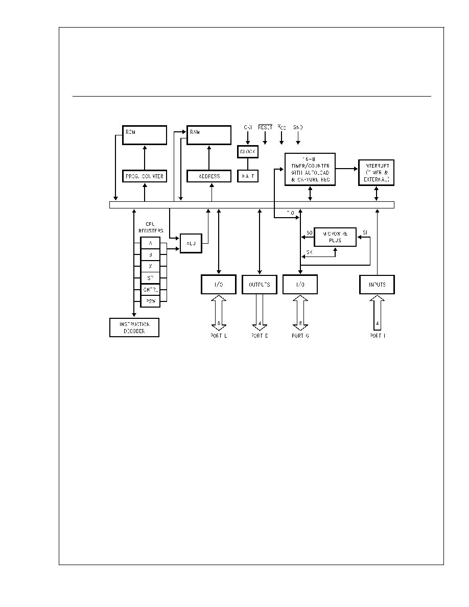
Block Diagram
DS009103-1
FIGURE 1.
COP820C/COP840C
www.national.com
2
COP920C/COP922C/COP940C/COP942C
Absolute Maximum Ratings
(Note 1)
If Military/Aerospace specified devices are required,
please contact the National Semiconductor Sales Office/
Distributors for availability and specifications.
Supply Voltage (V
CC
)
7V
Voltage at any Pin
-0.3V to V
CC
+ 0.3V
Total Current into V
CC
Pin (Source)
50 mA
Total Current out of GND Pin (Sink)
60 mA
Storage Temperature Range
-65∞C to +140∞C
Note 1:
Absolute maximum ratings indicate limits beyond which damage to
the device may occur. DC and AC electrical specifications are not ensured
when operating the device at absolute maximum ratings.
DC Electrical Characteristics
COP92XC, COP94XC; 0∞C
T
A
+70∞C unless otherwise specified
Parameter
Condition
Min
Typ
Max
Units
Operating Voltage
COP9XXC
2.3
4.0
V
COP9XXCH
4.0
6.0
V
Power Supply Ripple (Note 2)
Peak to Peak
0.1 V
CC
V
Supply Current (Note 3)
CKI = 10 MHz
V
CC
= 6V, tc = 1 µs
6.0
mA
CKI = 4 MHz
V
CC
= 6V, tc = 2.5 µs
4.0
mA
CKI = 4 MHz
V
CC
= 4V, tc = 2.5 µs
2.0
mA
CKI = 1 MHz
V
CC
= 4V, tc = 10 µs
1.2
mA
HALT Current
V
CC
= 6V, CKI = 0 MHz
<
0.7
8.0
µA
(Note 4)
V
CC
= 4V, CKI = 0 MHz
<
0.4
5.0
µA
Input Levels
RESET , CKI
Logic High
0.9 V
CC
V
Logic Low
0.1 V
CC
V
All Other Inputs
Logic High
0.7 V
CC
V
Logic Low
0.2 V
CC
V
Hi-Z Input Leakage
V
CC
= 6.0V
-1
+1
µA
Input Pullup Current
V
CC
= 6.0V, V
IN
= 0V
-40
-250
µA
G Port Input Hysteresis
0.35 V
CC
V
Output Current Levels
D Outputs
Source
V
CC
= 4.5V, V
OH
= 3.8V
-0.4
mA
V
CC
= 2.3V, V
OH
= 1.6V
-0.2
mA
Sink
V
CC
= 4.5V, V
OL
= 1.0V
10
mA
V
CC
= 2.3V, V
OL
= 0.4V
2
mA
All Others
Source (Weak Pull-Up)
V
CC
= 4.5V, V
OH
= 3.2V
-10
-110
µA
V
CC
= 2.3V, V
OH
= 1.6V
-2.5
-33
µA
Source (Push-Pull Mode)
V
CC
= 4.5V, V
OH
= 3.8V
-0.4
mA
V
CC
= 2.3V, V
OH
= 1.6V
-0.2
Sink (Push-Pull Mode)
V
CC
= 4.5V, V
OL
= 0.4V
1.6
mA
V
CC
= 2.3V, V
OL
= 0.4V
0.7
TRI-STATE Leakage
V
CC
= 6.0V
-1.0
+1.0
µA
Allowable Sink/Source
Current Per Pin
D Outputs (Sink)
15
mA
All Others
3
mA
Maximum Input Current (Note 5)
Without Latchup (Room Temp)
Room Temp
±
100
mA
COP820C/COP840C
www.national.com
3
DC Electrical Characteristics
(Continued)
COP92XC, COP94XC; 0∞C
T
A
+70∞C unless otherwise specified
Parameter
Condition
Min
Typ
Max
Units
RAM Retention Voltage, Vr
500 ns Rise and Fall Time (Min)
2.0
V
Input Capacitance
7
pF
Load Capacitance on D2
1000
pF
Note 2: Rate of voltage change must be less than 0.5V/ms.
Note 3: Supply current is measured after running 2000 cycles with a square wave CKI input, CKO open, inputs at rails and outputs open.
Note 4: The HALT mode will stop CKI from oscillating in the RC and the Crystal configurations. Test conditions: All inputs tied to V
CC
, L and G0 -- G5 configured as
outputs and set high. The D port set to zero.
Note 5: Except pin G7: +100 mA, -25 mA (COP920C only). Sampled and not 100% tested. Pins G6 and RESET are designed with a high voltage input network for
factory testing. These pins allow input voltages greater than V
CC
and the pins will have sink current to V
CC
when biased at voltages greater than V
CC
(the pins do
not have source current when biased at a voltage below V
CC
). The effective resistance to V
CC
is 750
(typical). These two pins will not latch up. The voltage at the
pins must be limited to less than 14V.
AC Electrical Characteristics
0∞C
T
A
+70∞C unless otherwise specified
Parameter
Condition
Min
Typ
Max
Units
Instruction Cycle Time (tc)
Ext., Crystal/Resonator
V
CC
4.0V
1
DC
µs
(Div-by 10)
2.3V
V
CC
4.0V
2.5
DC
µs
R/C Oscillator Mode
V
CC
4.0V
3
DC
µs
(Div-by 10)
2.3V
V
CC
4.0V
7.5
DC
µs
CKI Clock Duty Cycle (Note 6)
fr = Max
40
60
%
Rise Time (Note 6)
fr = 10 MHz Ext Clock
12
ns
Fall Time (Note 6)
fr = 10 MHz Ext Clock
8
ns
Inputs
t
SETUP
V
CC
4.0V
200
ns
2.3V
V
CC
4.0V
500
ns
t
HOLD
V
CC
4.0V
60
ns
2.3V
V
CC
4.0V
150
ns
Output Propagation Delay
C
L
= 100 pF, R
L
= 2.2 k
t
PD1
, t
PD0
SO, SK
V
CC
4.0V
0.7
µs
2.5V
V
CC
4.0V
1.75
µs
All Others
V
CC
4.0V
1
µs
2.5V
V
CC
4.0V
2.5
µs
MICROWIRE
TM
Setup Time (t
UWS
)
20
ns
MICROWIRE Hold Time (t
UWH
)
56
ns
MICROWIRE Output Propagation
Delay (t
UPD
)
220
ns
Input Pulse Width
Interrupt Input High Time
t
C
Interrupt Input Low Time
t
C
Timer Input High Time
t
C
Timer Input Low Time
t
C
Reset Pulse Width
1.0
µs
Note 6: Parameter sampled (not 100% tested).
COP820C/COP840C
www.national.com
4
COP820C/COP822C/COP840C/COP842C
Absolute Maximum Ratings
(Note 7)
If Military/Aerospace specified devices are required,
please contact the National Semiconductor Sales Office/
Distributors for availability and specifications.
Supply Voltage (V
CC
)
7V
Voltage at any Pin
-0.3V to V
CC
+ 0.3V
Total Current into V
CC
Pin (Source)
50 mA
Total Current out of GND Pin (Sink)
60 mA
Storage Temperature Range
-65∞C to +140∞C
Note 7:
Absolute maximum ratings indicate limits beyond which damage to
the device may occur. DC and AC electrical specifications are not ensured
when operating the device at absolute maximum ratings.
DC Electrical Characteristics
COP82XC, COP84XC; -40∞C
T
A
+85∞C unless otherwise specified
Parameter
Condition
Min
Typ
Max
Units
Operating Voltage
2.5
6.0
V
Power Supply Ripple (Note 8)
Peak to Peak
0.1 V
CC
V
Supply Current (Note 9)
CKI = 10 MHz
V
CC
= 6V, tc = 1 µs
6.0
mA
CKI = 4 MHz
V
CC
= 6V, tc = 2.5 µs
4.0
mA
CKI = 4 MHz
V
CC
= 4.0V, tc = 2.5 µs
2.0
mA
CKI = 1 MHz
V
CC
= 4.0V, tc = 10 µs
1.2
mA
HALT Current (Note 10)
V
CC
= 6V, CKI = 0 MHz
<
1
10
µA
Input Levels
RESET , CKI
Logic High
0.9 V
CC
V
Logic Low
0.1 V
CC
V
All Other Inputs
Logic High
0.7 V
CC
V
Logic Low
0.2 V
CC
V
Hi-Z Input Leakage
V
CC
= 6.0V
-2
+2
µA
Input Pullup Current
V
CC
= 6.0V, V
IN
= 0V
-40
-250
µA
G Port Input Hysteresis
0.35 V
CC
V
Output Current Levels
D Outputs
Source
V
CC
= 4.5V, V
OH
= 3.8V
-0.4
mA
V
CC
= 2.5V, V
OH
= 1.8V
-0.2
mA
Sink
V
CC
= 4.5V, V
OL
= 1.0V
10
mA
V
CC
= 2.5V, V
OL
= 0.4V
2
mA
All Others
Source (Weak Pull-Up)
V
CC
= 4.5V, V
OH
= 3.2V
-10
-110
µA
V
CC
= 2.5V, V
OH
= 1.8V
-2.5
-33
µA
Source (Push-Pull Mode)
V
CC
= 4.5V, V
OH
= 3.8V
-0.4
mA
V
CC
= 2.5V, V
OH
= 1.8V
-0.2
Sink (Push-Pull Mode)
V
CC
= 4.5V, V
OL
= 0.4V
1.6
mA
V
CC
= 2.5V, V
OL
= 0.4V
0.7
TRI-STATE Leakage
-2.0
+2.0
µA
Allowable Sink/Source
Current Per Pin
D Outputs (Sink)
15
mA
All Others
3
mA
Maximum Input Current (Note 11)
Without Latchup (Room Temp)
Room Temp
±
100
mA
RAM Retention Voltage, Vr
500 ns Rise and Fall Time
(Min)
2.0
V
Input Capacitance
7
pF
COP820C/COP840C
www.national.com
5