COP8ACC Family
8-Bit CMOS ROM Based and OTP Microcontrollers with
4k or 16k Memory and High Resolution A/D
General Description
The COP8ACC Family ROM based microcontrollers are
highly integrated COP8
TM
Feature core devices with 4k
memory and advanced features including a High-Resolution
A/D. These single-chip CMOS devices are suited for appli-
cations requiring a full featured, low EMI controller with an
A/D (only one external capacitor required). COP8ACC7 de-
vices are pin and software compatible (different V
CC
range)
16k OTP EPROM versions for pre-production. Erasable win-
dowed versions are available for use with a range of COP8
software and hardware development tools.
Family features include an 8-bit memory mapped architec-
ture, 4 MHz CKI with 2.5µs instruction cycle, 6 channel A/D
with 12-bit resolution, analog capture timer, analog current
source and V
CC
/2 reference, one multi-function 16-bit timer/
counter, MICROWIRE/PLUS serial I/O, two power saving
HALT/IDLE modes, MIWU, high current outputs, software
selectable I/O options, WATCHDOG
TM
timer and Clock Moni-
tor, Low EMI 2.5V to 5.5V operation and 20/28 pin packages.
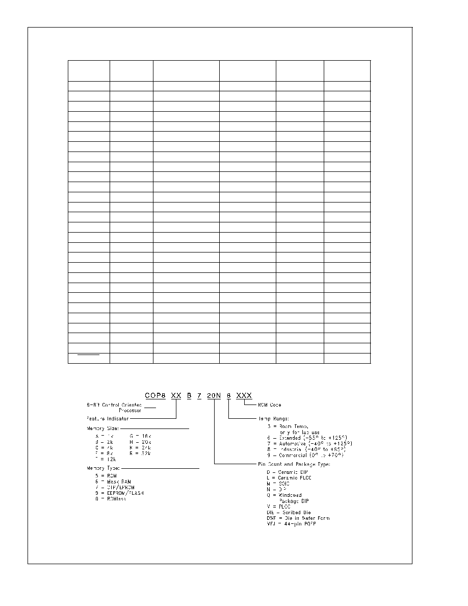
Devices included in this datasheet are:
Device
Memory (bytes)
RAM (bytes)
I/O Pins
Packages
Temperature
COP8ACC5xxx9
4k ROM
128
15/23
20 SOIC, 28 DIP/SOIC
0 to +70∞C
COP8ACC5xxx8
4k ROM
128
15/23
20 SOIC, 28 DIP/SOIC
-40 to +85∞C
COP8ACC7xxx9
16k OTP EPROM
128
15/23
20 SOIC, 28 DIP/SOIC
0 to +70∞C
COP8ACC7xxx8
16k OTP EPROM
128
15/23
20 SOIC, 28 DIP/SOIC
-40 to +85∞C
Key Features
n
Analog Function Block with 12-bit A/D including
-- Analog comparator with seven input mux
-- Constant Current Source and V
CC/2
Reference
-- 16-bit capture timer (upcounter) clocked from CKI
with auto reset on timer startup
n
Quiet design (reduced radiated emissions)
n
4096 bytes on-board ROM or 16,384 OTP EPROM with
security feature
n
128 bytes on-board RAM
Additional Peripheral Features
n
Idle Timer
n
One 16-bit timer with two 16-bit registers supporting:
-- Processor Independent PWM mode
-- External Event counter mode
-- Input Capture mode
n
Multi-Input Wake-Up (MIWU) with optional interrupts
n
WATCHDOG and clock monitor logic
n
MICROWIRE/PLUS
TM
serial I/O with programmable shift
clock-polarity
I/O Features
n
Software selectable I/O options (Push-Pull Output, Weak
Pull-Up Input, High Impedance Input)
n
High current outputs
n
Schmitt Trigger inputs on ports G and L
n
Packages: 28 DIP/SO with 23 I/O pins,
20 SO with 15 I/O pins
CPU/Instruction Set Features
n
2.5 µs instruction cycle time
n
Eight multi-source vectored interrupt servicing
-- External Interrupt
-- Idle Timer T0
-- Timer T1 associated Interrupts
-- MICROWIRE/PLUS
-- Multi-Input Wake Up
-- Software Trap
-- Default VIS
-- A/D (Capture Timer)
n
8-bit Stack Pointer (SP) -- stack in RAM
n
Two 8-bit Registers Indirect Data Memory Pointers
(B and X)
Fully Static CMOS
n
Two power saving modes: HALT and IDLE
n
Single supply operation: 2.5V to 5.5V for COP8ACC5
n
Single supply operation: 2.7V to 5.5V for COP8ACC7
n
Temperature ranges: 0∞C to +70∞C, -40∞C to +85∞C
Development System
n
Emulation and OTP devices
n
Real time emulation and full program debug offered by
MetaLink development system
Applications
n
Battery Chargers
n
Appliances
n
Data Acquisition systems
COP8
TM
, MICROWIRE
TM
, MICROWIRE/PLUS
TM
, and WATCHDOG
TM
are trademarks of National Semiconductor Corporation.
TRI-STATE
Æ
is a registered trademark of National Semiconductor Corporation.
iceMASTER
Æ
is a registered trademark of MetaLink Corporation.
July 2000
COP8ACC
Family
8-Bit
CMOS
ROM
Based
and
OTP
Microcontrollers
with
4k
or
16k
Memory
and
High
Resolution
A/D
© 2001 National Semiconductor Corporation
DS012865
www.national.com
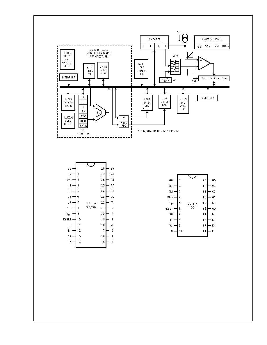
Block Diagram
Connection Diagrams
DS012865-1
FIGURE 1. Block Diagram
DS012865-2
Top View
Order Number COP8ACC528N9 or COP8ACC528N8
See NS Molded Package Number N28A
Order Number COP8ACC528M9 or COP8ACC528M8
Order Number COP8ACC728N9-XE or
COP8ACC728N8-XE
Order Number COP8ACC728M9-XE or
COP8ACC728M8-XE
See NS Molded Package Number M28B
DS012865-3
Note: -X Crystal Oscillator
Note: -E Halt Enable
Top View
Order Number COP8ACC520M9 or COP8ACC520N8
Order Number COP8ACC720M9-XE or
COP8ACC720N8-XE
See NS Molded Package Number M20B
FIGURE 2. Connection Diagrams
COP8ACC
Family
www.national.com
2
Absolute Maximum Ratings
(Note 1)
If Military/Aerospace specified devices are required,
please contact the National Semiconductor Sales Office/
Distributors for availability and specifications.
Supply Voltage (V
CC
)
7V
Voltage at Any Pin
-0.3V to V
CC
+0.3V
Total Current into V
CC
Pin (Source)
100 mA
Total Current out of GND Pin (Sink)
110 mA
Storage Temperature Range
-65∞C to +140∞C
Note 1: Absolute maximum ratings indicate limits beyond which damage to
the device may occur. DC and AC electrical specifications are not ensured
when operating the device at absolute maximum ratings.
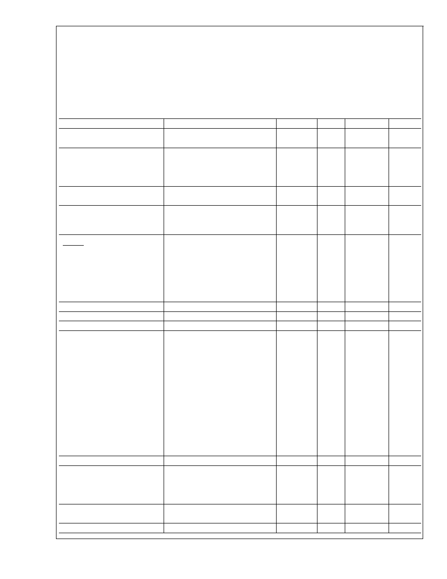
DC Electrical Characteristics
0∞C
T
A
+70∞C unless otherwise specified [OTP Value]
Parameter
Conditions
Min
Typ
Max
Units
Operating Voltage
Peak-to-Peak
2.5 [2.7]
5.5
V
Power Supply Ripple (Note 2)
0.1 V
CC
V
Supply Current (Note 3)
CKI = 4 MHz
V
CC
= 5.5V, t
C
= 2.5 µs
5.5 [9.5]
mA
CKI = 4 MHz
V
CC
= 4V, t
C
= 2.5 µs
2.5 [6.5]
mA
CKI = 1 MHz
V
CC
= 4V, t
C
= 10 µs
1.4 [5.4]
mA
HALT Current (Note 4)
V
CC
= 5.5V, CKI = 0 MHz
<
5
8 [10]
µA
V
CC
= 4V, CKI = 0 MHz
<
3
4 [6]
µA
IDLE Current
CKI = 4 MHz
V
CC
= 5.5V, t
C
= 2.5 µs
1.5
mA
CKI = 1 MHz
V
CC
= 4V, t
C
= 10 µs
0.5
mA
Input Levels (V
IH
, V
IL
)
RESET
Logic High
0.8 V
CC
V
Logic Low
0.2 V
CC
V
CKI, All Other Inputs
Logic High
0.7 V
CC
V
Logic Low
0.2 V
CC
V
Hi-Z Input Leakage
V
CC
= 5.5V
1
1
µA
Input Pullup Current
V
CC
= 5.5V, V
IN
= 0V
-40
-250
µA
G and L Port Input Hysteresis
(Note 6)
0.35 V
CC
V
Output Current Levels
D Outputs
Source
V
CC
= 4V, V
OH
= 3.3V
-0.4
mA
V
CC
= 2.5V [2.7V], V
OH
= 1.8V
-0.2
mA
Sink
V
CC
= 4V, V
OL
= 1V
10
mA
V
CC
= 2.5V [2.7V], V
OL
= 0.4V
2.0
mA
All Others
Source (Weak Pull-Up Mode)
V
CC
= 4V, V
OH
= 2.7V
-10
-110
µA
V
CC
= 2.5V [2.7V], V
OH
= 1.8V
-2.5
-33
µA
Source (Push-Pull Mode)
V
CC
= 4V, V
OH
= 3.3V
-0.4
mA
V
CC
= 2.5V [2.7V], V
OH
= 1.8V
-0.2
mA
Sink (Push-Pull Mode)
V
CC
= 4V, V
OL
= 0.4V
1.6
mA
V
CC
= 2.5V [2.7V], V
OL
= 0.4V
0.7
mA
TRI-STATE
Æ
Leakage
V
CC
= 5.5V
1
1
µA
Allowable Sink/Source
Current per Pin
D Outputs (Sink)
15
mA
All others
3
mA
Maximum Input Current
Room Temp
±
200
mA
without Latchup (Note 5)
RAM Retention Voltage, V
r
500 ns Rise and Fall Time (min)
2
V
COP8ACC
Family
www.national.com
4

DC Electrical Characteristics
(Continued)
0∞C
T
A
+70∞C unless otherwise specified [OTP Value]
Parameter
Conditions
Min
Typ
Max
Units
Input Capacitance
(Note 6)
7
pF
Load Capacitance on D2
(Note 6)
1000
pF
AC Electrical Characteristics
0∞C
T
A
+70∞C unless otherwise specified [OTP Value]
Parameter
Conditions
Min
Typ
Max
Units
Instruction Cycle Time (t
C
)
Crystal, Resonator
2.5V, [2.7V]
V
CC
4V
2.5
DC
µs
4V
V
CC
5.5V
1.0
DC
µs
R/C Oscillator
2.5V, [2.7V]
V
CC
4V
7.5
DC
µs
4V
V
CC
5.5V
3.0
DC
µs
Inputs
t
SETUP
4V
V
CC
5.5V
200
ns
2.5V, [2.7V]
V
CC
4V
500
ns
t
HOLD
4V
V
CC
5.5V
60
ns
2.5V, [2.7V]
V
CC
4V
150
ns
Output Propagation Delay (Note 6)
R
L
= 2.2k, C
L
= 100 pF
t
PD1
, t
PD0
SO, SK
4V
V
CC
5.5V
0.7
µs
2.5V, [2.7V]
V
CC
4V
1.75
µs
All Others
4V
V
CC
5.5V
1
µs
2.5V, [2.7V]
V
CC
4V
2.5
µs
MICROWIRE
TM
Setup Time (t
UWS
) (Note
6)
V
CC
4V
20
ns
MICROWIRE Hold Time (t
UWH
) (Note 6)
V
CC
4V
56
ns
MICROWIRE Output Propagation Delay
(t
UPD
)
V
CC
4V
220
ns
Input Pulse Width (Note 7)
Interrupt Input High Time
1
t
C
Interrupt Input Low Time
1
t
C
Timer 1, 2, 3 Input High Time
1
t
C
Timer 1, 2, 3 Input Low Time
1
t
C
Reset Pulse Width
1
µs
Note 2: Maximum rate of voltage change must be
<
0.5V/ms.
Note 3: Supply current is measured after running 2000 cycles with a square wave CKI input, CKO open, inputs at rails and outputs open.
Note 4: The HALT mode will stop CKI from oscillating in the RC and the Crystal configurations. Measurement of I
DD
HALT is done with device neither sourcing or
sinking current; with L, C, and G0≠G5 programmed as low outputs and not driving a load; all outputs programmed low and not driving a load; all inputs tied to V
CC
;
clock monitor and comparator disabled. Parameter refers to HALT mode entered via setting bit 7 of the G Port data register. Part will pull up CKI during HALT in
crystal clock mode.
Note 5: Pins G6 and RESET are designed with a high voltage input network. These pins allow input voltages
>
V
CC
and the pins will have sink current to V
CC
when
biased at voltages
>
V
CC
(the pins do not have source current when biased at a voltage below V
CC
). The effective resistance to V
CC
is 750
(typical). These two
pins will not latch up. The voltage at the pins must be limited to less than 14V. WARNING: Voltages in excess of 14V will cause damage to the pins. This warning
excludes ESD transients.
Note 6: The output propagation delay is referenced to the end of the instruction cycle where the output change occurs.
Note 7: Parameter characterized but not tested.
Note 8: t
C
= Instruction Cycle Time.
COP8ACC
Family
www.national.com
5