TL L 8338
DM54LS450DM74LS450
161
Multiplexer
PRELIMINARY
July 1989
DM54LS450 DM74LS450 16 1 Multiplexer
General Description
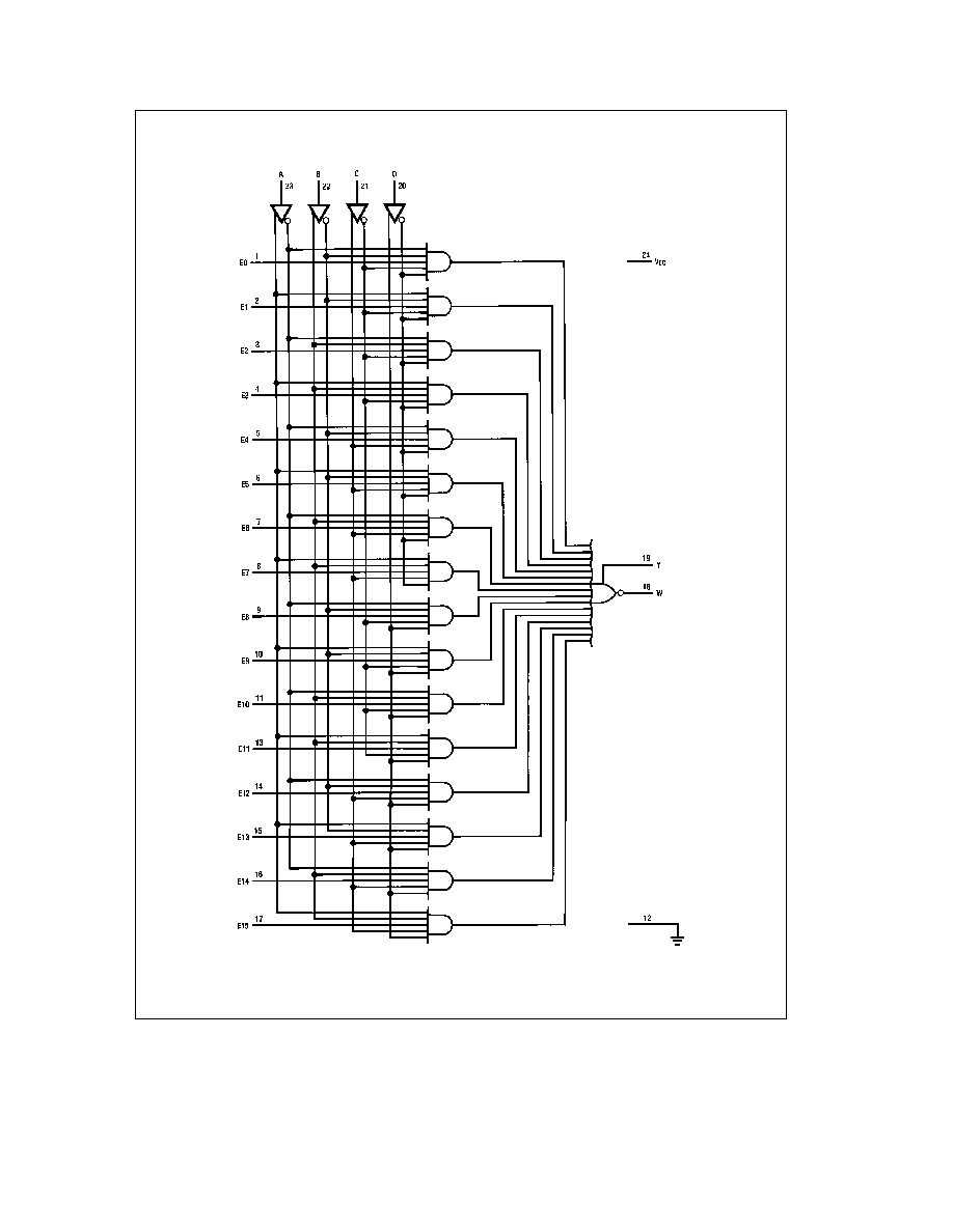
The 16 1 Mux selects one of sixteen inputs E0 through E15
specified by four binary select inputs A B C and D The
true data is output on Y and the inverted data on W Propa-
gation delays are the same for both inputs and addresses
and are specified for 50 pF loading Outputs conform to the
standard 8 mA LS totem pole drive standard
Features Benefits
Y
24-pin SKINNYDIP saves space
Y
Similar to 74150 (Fat DIP)
Y
Low current PNP inputs reduce loading
Connection Diagram
Top View
TL L 8338 ≠ 1
Order Number DM54LS450J DM74LS450J
DM74LS450N or DM74LS450V
See NS Package Number J24F N24C or V28A
Standard Test Load
TL L 8338 ≠ 2
Function Table
Input
Output
Select
D
C
B
A
W
Y
L
L
L
L
E0
E0
L
L
L
H
E1
E1
L
L
H
L
E2
E2
L
L
H
H
E3
E3
L
H
L
L
E4
E4
L
H
L
H
E5
E5
L
H
H
L
E6
E6
L
H
H
H
E7
E7
H
L
L
L
E8
E8
H
L
L
H
E9
E9
H
L
H
L
E10
E10
H
L
H
H
E11
E11
H
H
L
L
E12
E12
H
H
L
H
E13
E13
H
H
H
L
E14
E14
H
H
H
H
E15
E15
C1995 National Semiconductor Corporation
RRD-B30M115 Printed in U S A
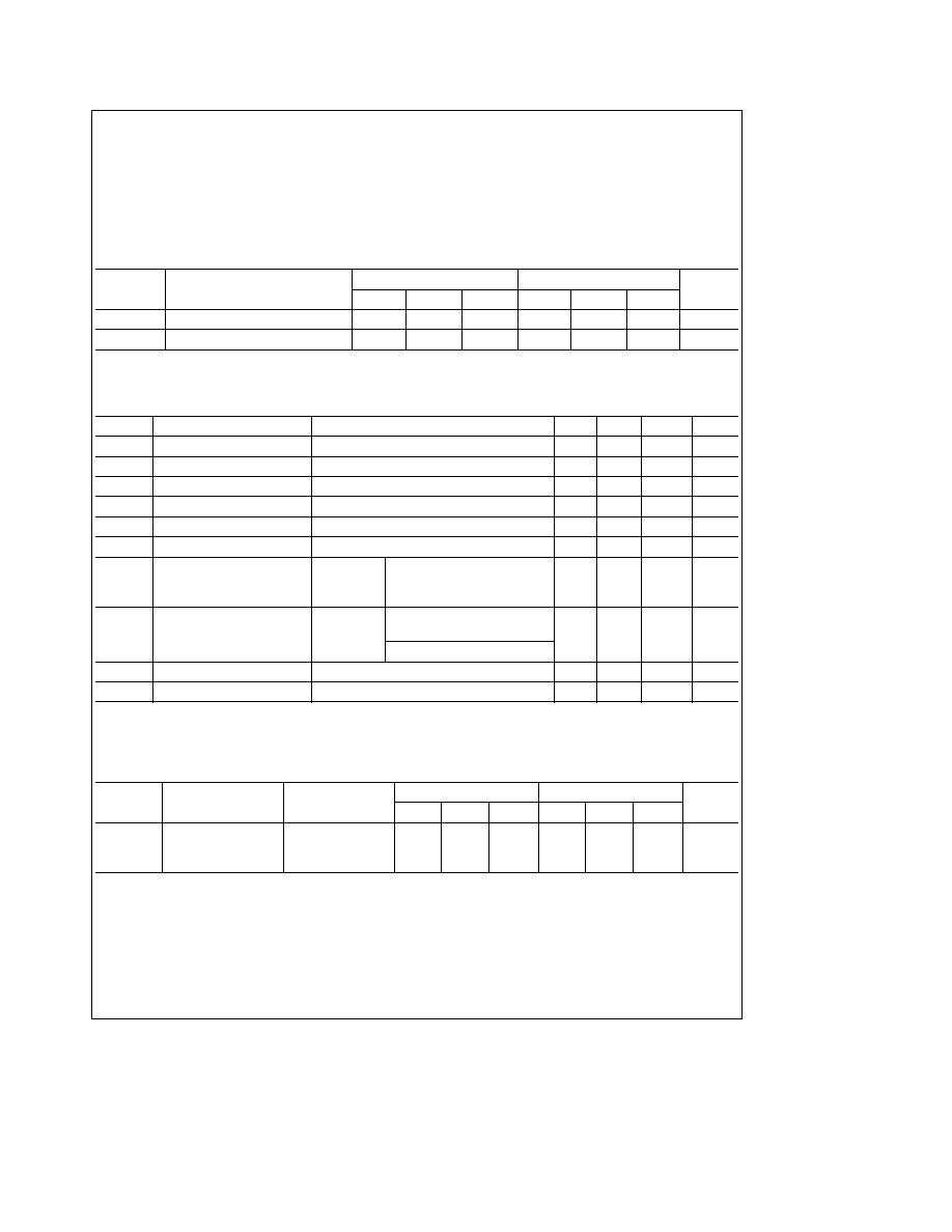
Absolute Maximum Ratings
If Military Aerospace specified devices are required
please contact the National Semiconductor Sales
Office Distributors for availability and specifications
Supply Voltage V
CC
7V
Input Voltage
5 5V
Off-State Output Voltage
5 5V
Storage Temperature
b
65 to
a
150 C
Operating Conditions
Symbol
Parameter
Military
Commercial
Units
Min
Nom
Max
Min
Nom
Max
V
CC
Supply Voltage
4 5
5
5 5
4 75
5
5 25
V
T
A
Operating Free-Air Temperature
b
55
125
0
75
C
Case temperature
Electrical Characteristics
Over Operating Conditions
Symbol
Parameter
Test Conditions
Min
Typ
Max
Units
V
IL
Low-Level Input Voltage
0 8
V
V
IH
High-Level Input Voltage
2
V
V
IC
Input Clamp Voltage
V
CC
e
MIN
I
I
e b
18 mA
b
1 5
V
I
IL
Low-Level Input Current
V
CC
e
MAX
V
I
e
0 4V
b
0 25
mA
I
IH
High-Level Input Current
V
CC
e
MAX
V
I
e
2 4V
25
m
A
I
I
Maximum Input Current
V
CC
e
MAX
V
I
e
5 5V
1
mA
V
CC
e
MIN
V
OL
Low-Level Output Voltage
V
IL
e
0 8V
I
OL
e
8 mA
0 5
V
V
IH
e
2V
V
CC
e
MIN
MIL
I
OH
e b
2 mA
V
OH
High-Level Output Voltage
V
IL
e
0 8V
2 4
V
V
IH
e
2V
COM
I
OH
e b
3 2 mA
I
OS
Output Short-Circuit Current
V
CC
e
5 0V
V
O
e
0V
b
30
b
130
mA
I
CC
Supply Current
V
CC
e
MAX
60
100
mA
No more than one output should be shorted at a time and duration of the short-circuit should not exceed one second
All typical values are at V
CC
e
5V T
A
e
25 C
Switching Characteristics
Over Operating Conditions
Symbol
Parameter
Test Conditions
Military
Commercial
Units
(See Test Load)
Min
Typ
Max
Min
Typ
Max
C
L
e
50 pF
t
PD
Any Input to Y or W
R
1
e
560X
25
45
25
40
ns
R
2
e
1 1kX
2
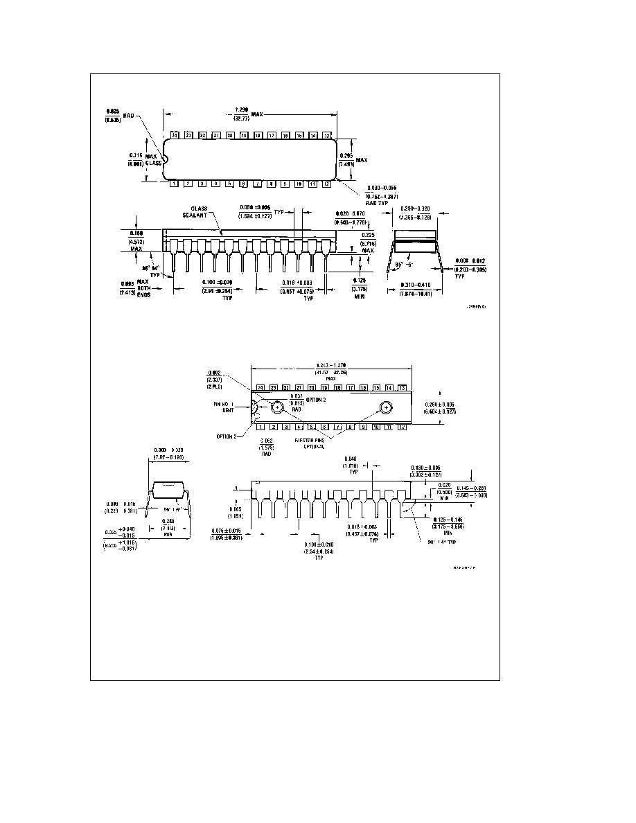
Physical Dimensions
inches (millimeters)
24-Pin Narrow Ceramic Dual-In-Line Package (J)
Order Number DM54LS450J or DM74LS450J
NS Package Number J24F
24-Pin Narrow Plastic Dual-In-Line Package (N)
Order Number DM74LS450N
NS Package Number N24C
5