 | ÐлекÑÑоннÑй компоненÑ: DM54S194 | СкаÑаÑÑ:  PDF PDF  ZIP ZIP |
Äîêóìåíòàöèÿ è îïèñàíèÿ www.docs.chipfind.ru
TL F 6475
DM54S194DM74S194
4-Bit
Bidirectional
Universal
Shift
Registers
June 1989
DM54S194 DM74S194
4-Bit Bidirectional Universal Shift Registers
General Description
These bidirectional shift registers are designed to incorpo-
rate virtually all of the features a system designer may want
in a shift register they feature parallel inputs parallel out-
puts right-shift and left-shift serial inputs operating-mode-
control inputs and a direct overriding clear line The register
has four distinct modes of operation namely
Parallel (broadside) load
Shift right (in the direction Q
A
toward Q
D
)
Shift left (in the direction Q
D
toward Q
A
)
Inhibit clock (do nothing)
Synchronous parallel loading is accomplished by applying
the four bits of data and taking both mode control inputs S0
and S1 high The data are loaded into the associated flip-
flops and appear at the outputs after the positive transition
of the clock input During loading serial data flow is inhibit-
ed
Shift right is accomplished synchronously with the rising
edge of the clock pulse when S0 is high and S1 is low
Serial data for this mode is entered at the shift-right data
input When S0 is low and S1 is high data shifts left syn-
chronously and new data is entered at the shift-left serial
input
Clocking of the flip-flop is inhibited when both mode control
inputs are low
Features
Y
Parallel inputs and outputs
Y
Four operating modes
Synchronous parallel load
Right shift
Left shift
Do nothing
Y
Positive edge-triggered clocking
Y
Direct overriding clear
Y
Typical clock frequency 105 MHz
Y
Typical power dissipation 425 mW
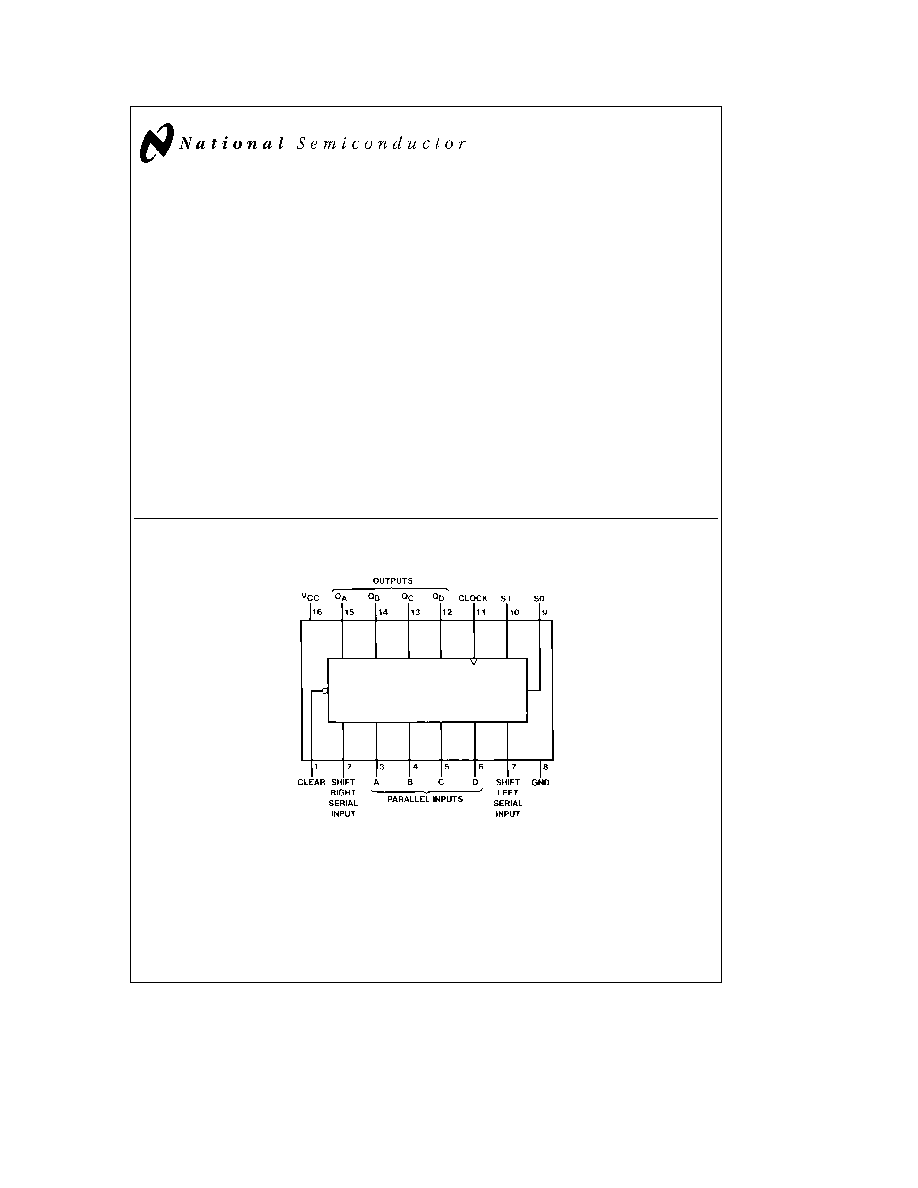
Connection Diagram
Dual-In-Line Package
TL F 6475 1
Order Number DM54S194J or DM74S194N
See NS Package Number J16A or N16E
C1995 National Semiconductor Corporation
RRD-B30M105 Printed in U S A
Absolute Maximum Ratings
(Note)
If Military Aerospace specified devices are required
please contact the National Semiconductor Sales
Office Distributors for availability and specifications
Supply Voltage
7V
Input Voltage
5 5V
Operating Free Air Temperature Range
DM54S
b
55 C to
a
125 C
DM74S
0 C to
a
70 C
Storage Temperature Range
b
65 C to
a
150 C
Note
The ``Absolute Maximum Ratings'' are those values
beyond which the safety of the device cannot be guaran-
teed The device should not be operated at these limits The
parametric values defined in the ``Electrical Characteristics''
table are not guaranteed at the absolute maximum ratings
The ``Recommended Operating Conditions'' table will define
the conditions for actual device operation
Recommended Operating Conditions
Symbol
Parameter
DM54S194
DM74S194
Units
Min
Nom
Max
Min
Nom
Max
V
CC
Supply Voltage
4 5
5
5 5
4 75
5
5 25
V
V
IH
High Level Input Voltage
2
2
V
V
IL
Low Level Input Voltage
0 8
0 8
V
I
OH
High Level Output Current
b
1
b
1
mA
I
OL
Low Level Output Current
20
20
mA
f
CLK
Clock Frequency (Note 1)
0
105
70
0
105
70
MHz
f
CLK
Clock Frequency (Note 2)
0
90
60
0
90
60
MHz
t
W
Pulse Width
Clock
7
7
ns
(Note 3)
Clear
12
12
t
SU
Setup Time
Mode
11
11
ns
(Note 3)
Data
5
5
t
H
Hold Time (Note 3)
3
3
ns
t
REL
Clear Release Time (Note 3)
9
9
ns
T
A
Free Air Operating Temperature
b
55
125
0
70
C
Note 1
C
L
e
15 pF R
L
e
280X T
A
e
25 C and V
CC
e
5V
Note 2
C
L
e
50 pF R
L
e
280X T
A
e
25 C and V
CC
e
5V
Note 3
T
A
e
25 C and V
CC
e
5V
Electrical Characteristics
over recommended operating free air temperature (unless otherwise noted)
Symbol
Parameter
Conditions
Min
Typ
Max
Units
(Note 4)
V
I
Input Clamp Voltage
V
CC
e
Min I
I
e b
18 mA
b
1 2
V
V
OH
High Level Output
V
CC
e
Min I
OH
e
Max
DM54
2 5
3 4
V
Voltage
V
IL
e
Max V
IH
e
Min
DM74
2 7
3 4
V
OL
Low Level Output
V
CC
e
Min I
OL
e
Max
0 5
V
Voltage
V
IH
e
Min V
IL
e
Max
I
I
Input Current
Max
V
CC
e
Max V
I
e
5 5V
1
mA
Input Voltage
I
IH
High Level Input Current
V
CC
e
Max V
I
e
2 7V
50
m
A
I
IL
Low Level Input Current
V
CC
e
Max V
I
e
0 5V
b
2
mA
I
OS
Short Circuit
V
CC
e
Max
DM54
b
40
b
100
mA
Output Current
(Note 5)
DM74
b
40
b
100
I
CC
Supply Current
V
CC
e
Max (Note 6)
85
135
mA
Note 4
All typicals are at V
CC
e
5V T
A
e
25 C
Note 5
Not more than one output should be shorted at a time and the duration should not exceed one second
Note 6
With all outputs open inputs A through D grounded and 4 5V applied to S0 S1 CLEAR and the SERIAL inputs I
CC
is tested with a momentary ground
then 4 5V applied to CLOCK
2
Switching Characteristics
at V
CC
e
5V and T
A
e
25 C (See Section 1 for Test Waveforms and Output Load)
From (Input)
R
L
e
280X
Symbol
Parameter
To (Output)
C
L
e
15 pF
C
L
e
50 pF
Units
Min
Max
Min
Max
f
MAX
Maximum Clock Frequency
70
60
MHz
t
PLH
Propagation Delay Time
Clock
12
15
ns
Low to High Level Output
to Q
t
PHL
Propagation Delay Time
Clock
16 5
20
ns
High to Low Level Output
to Q
t
PHL
Propagation Delay Time
Clear
18 5
23
ns
High to Low Level Output
to Q
Function Table
Inputs
Outputs
Clear
Mode
Clock
Serial
Parallel
Q
A
Q
B
Q
C
Q
D
S1
S0
Left
Right
A
B
C
D
L
X
X
X
X
X
X
X
X
X
L
L
L
L
H
X
X
L
X
X
X
X
X
X
Q
A0
Q
B0
Q
C0
Q
D0
H
H
H
u
X
X
a
b
c
d
a
b
c
d
H
L
H
u
X
H
X
X
X
X
H
Q
An
Q
Bn
Q
Cn
H
L
H
u
X
L
X
X
X
X
L
Q
An
Q
Bn
Q
Cn
H
H
L
u
H
X
X
X
X
X
Q
Bn
Q
Cn
Q
Dn
H
H
H
L
u
L
X
X
X
X
X
Q
Bn
Q
Cn
Q
Dn
L
H
L
L
X
X
X
X
X
X
X
Q
A0
Q
B0
Q
C0
Q
D0
H
e
High Level (steady state) L
e
Low Level (steady state) X
e
Don't Care (any input including transitions)
u
e
Transition from low to high level
a b c d
e
The level of steady state input at inputs A B C or D respectively
Q
A0
Q
B0
Q
C0
Q
D0
e
The level of Q
A
Q
B
Q
C
or Q
D
respectively before the indicated steady state input conditions were established
Q
An
Q
Bn
Q
Cn
Q
Dn
e
The level of Q
A
Q
B
Q
C
respectively before the most recent
u
transition of the clock
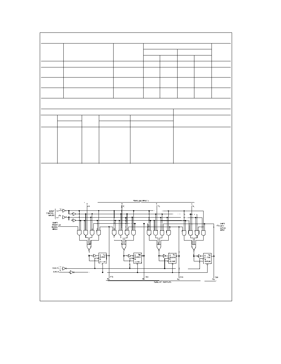
Logic Diagram
S194
TL F 6475 2
3
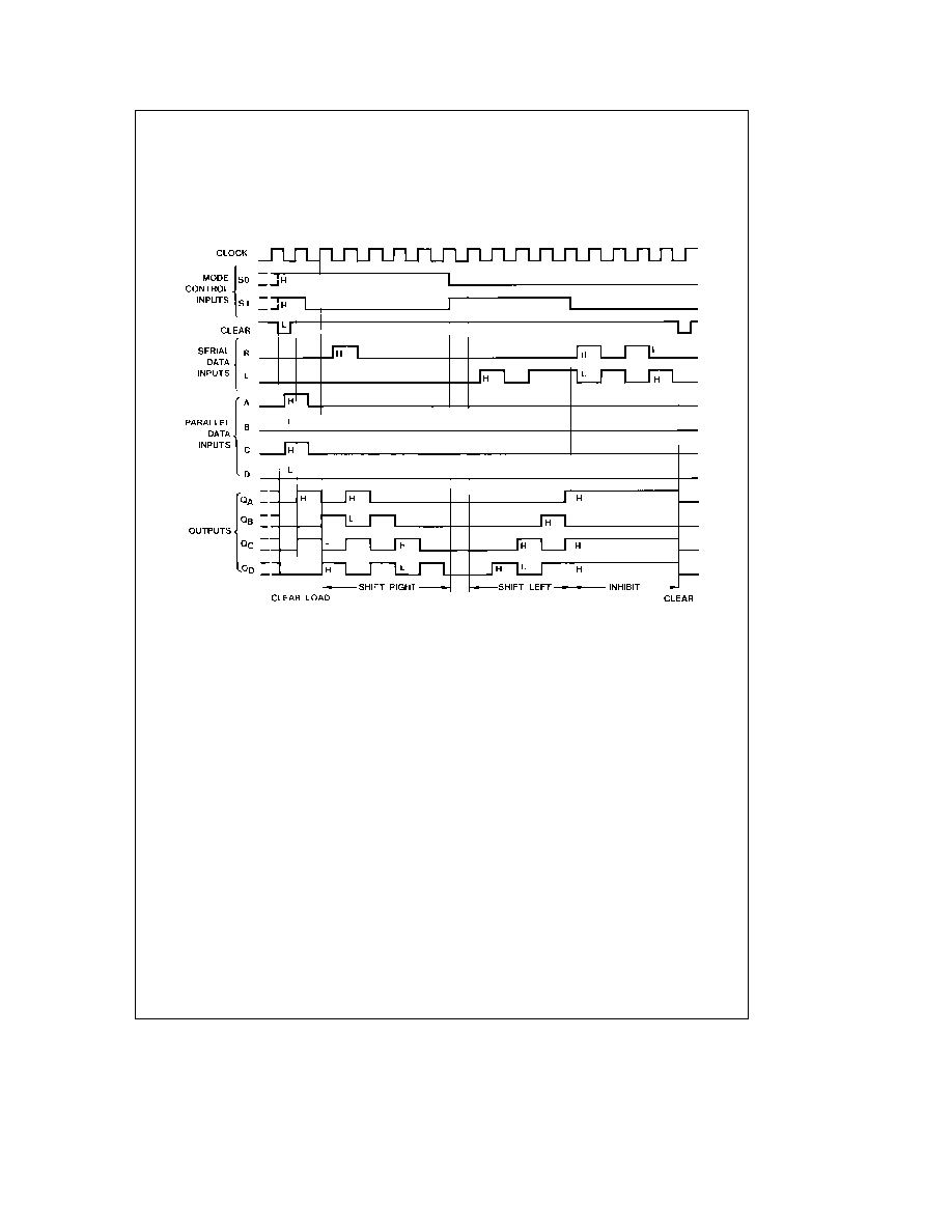
Timing Diagram
Typical Clear Load Right-Shift Left-Shift Inhibit and Clear Sequences
TL F 6475 3
4
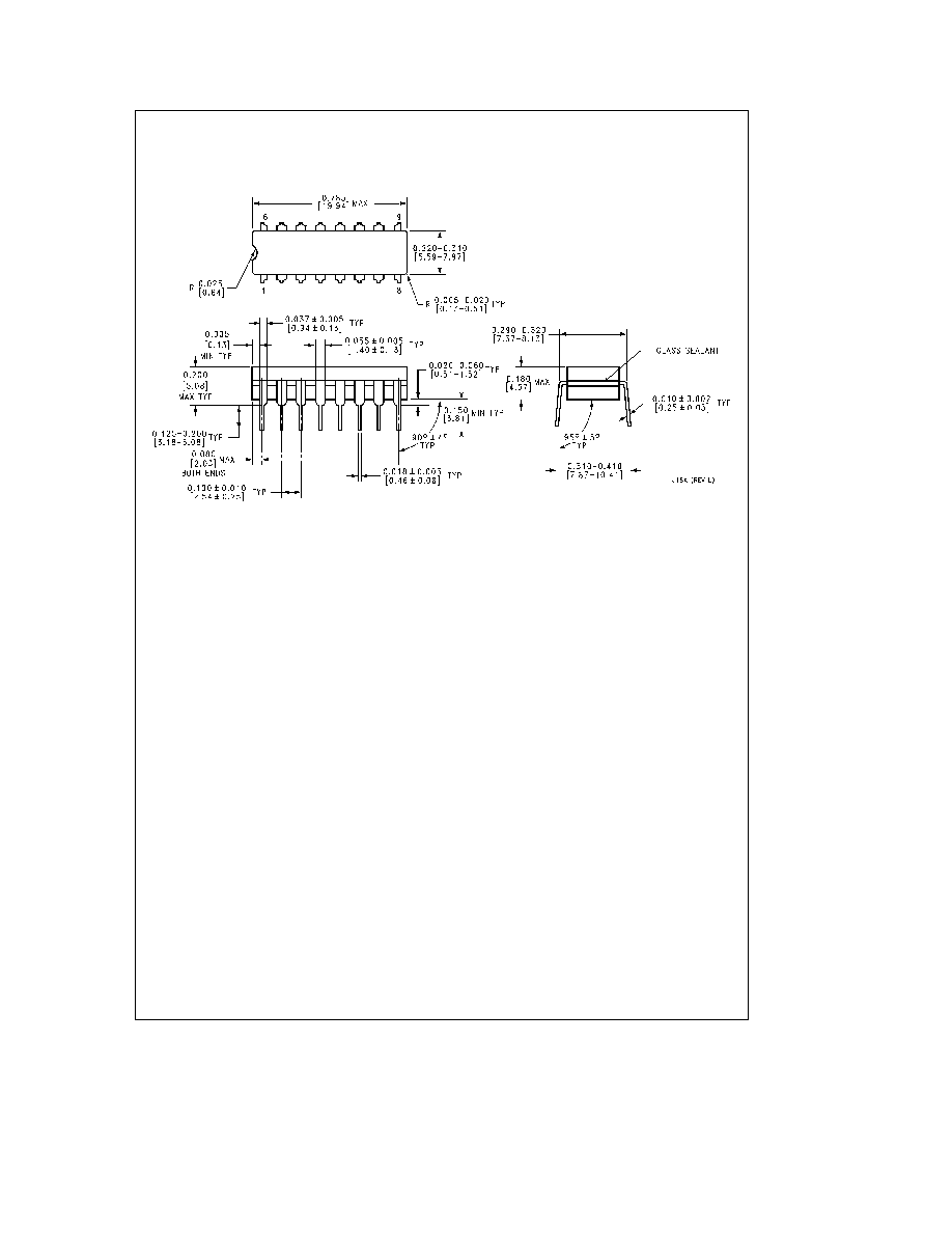
Physical Dimensions
inches (millimeters)
16-Lead Ceramic Dual-In-Line Package (J)
Order Number DM54S194J
NS Package Number J16A
5