
TL F 10185
DM74LS353
Dual
4-Input
Multiplexer
with
TRI-STATE
Outputs
February 1992
DM74LS353
Dual 4-Input Multiplexer with TRI-STATE
Outputs
General Description
The '353 is a dual 4-input multiplexer with TRI-STATE out-
puts It can select two bits of data from four sources using
common select inputs The outputs may be individually
switched to a high impedance state with a HIGH on the
respective Output (OE) inputs allowing the outputs to inter-
face directly with bus oriented systems It is fabricated with
the Schottky barrier diode process for high speed and is
completely compatible with all National TTL families
Features
Y
Inverted version of 'LS253
Y
Schottky process for high speed
Y
Multifunction capability
Connection Diagram
Dual-In-Line Package
TL F 10185 ≠ 1
Order Number DM74LS353M or DM74LS353N
See NS Package Number M16A or N16E
Logic Symbol
TL F 10185 ≠ 2
V
CC
e
Pin 16
GND
e
Pin 8
Pin Names
Description
I0a ≠ I3a
Side A Data Inputs
I0b ≠ I3b
Side B Data Inputs
S0 S1
Common Select Inputs
OE
a
Side A Output Enable Input (Active Low)
OE
b
Side B Output Enable Input (Active Low)
Z
a
Z
b
TRI-STATE Outputs (Inverted)
TRI-STATE
is a registered trademark of National Semiconductor Corporation
C1995 National Semiconductor Corporation
RRD-B30M105 Printed in U S A
Absolute Maximum Ratings
(Note)
Supply Voltage
7V
Input Voltage
7V
Operating Free Air Temperature Range
0 C to
a
70 C
Storage Temperature Range
b
65 C to
a
150 C
Note
The ``Absolute Maximum Ratings'' are those values
beyond which the safety of the device cannot be guaran-
teed The device should not be operated at these limits The
parametric values defined in the ``Electrical Characteristics''
table are not guaranteed at the absolute maximum ratings
The ``Recommended Operating Conditions'' table will define
the conditions for actual device operation
Recommended Operating Conditions
Symbol
Parameter
Min
Nom
Max
Units
V
CC
Supply Voltage
4 75
5
5 25
V
V
IH
High Level Input Voltage
2
V
V
IL
Low Level Input Voltage
0 8
V
I
OH
High Level Output Current
b
2 6
mA
I
OL
Low Level Output Current
24
mA
T
A
Free Air Operating Temperature
0
70
C
Electrical Characteristics
over recommended operating free air temperature range (unless otherwise noted)
Symbol
Parameter
Conditions
Min
Typ
Max
Units
(Note 1)
V
I
Input Clamp Voltage
V
CC
e
Min I
I
e b
18 mA
b
1 5
V
V
OH
High Level Output
V
CC
e
Min I
OH
e
Max
2 7
V
Voltage
V
IL
e
Max
V
OL
Low Level Output
V
CC
e
Min I
OL
e
Max
0 5
Voltage
V
IH
e
Min
V
I
OL
e
4 mA V
CC
e
Min
0 4
I
I
Input Current
Max
V
CC
e
Max V
I
e
7V
0 1
mA
Input Voltage
I
IH
High Level Input Current
V
CC
e
Max V
I
e
2 7V
20
m
A
I
IL
Low Level Input Current
V
CC
e
Max V
I
e
0 4V
b
0 4
mA
I
OS
Short Circuit Output Current
V
CC
e
Max (Note 2)
b
30
b
130
mA
I
CCL
Supply Current
V
CC
e
Max
12
mA
Outputs HIGH
In Sn OEn
e
GND
I
CCZ
Supply Current
V
CC
e
Max OEn
e
4 5V
14
mA
Outputs OFF
In Sn
e
GND
I
OZH
TRI ≠ STATE Output OFF
V
CC
e
V
CCH
20
m
A
Current HIGH
V
OZH
e
2 7V
I
OZL
TRI ≠ STATE Output OFF
V
CC
e
V
CCH
b
20
m
A
Current LOW
V
OZL
e
0 4V
Note 1
All typicals are at V
CC
e
5V T
A
e
25 C
Note 2
Not more than one output should be shorted at a time and the duration should not exceed one second
2

Switching Characteristics
V
CC
e a
5 0V T
A
e a
25 C
Symbol
Parameter
R
L
e
2 kX C
L
e
50 pF
Units
Min
Max
t
PLH
Propagation Delay
24
ns
t
PHL
Sn to Zn
32
t
PLH
Propagation Delay
15
ns
t
PHL
In to Zn
15
t
PZH
Output Enable Time
18
ns
t
PZL
OE to Zn
18
t
PHZ
Output Disable Time
18
ns
t
PLZ
OE to Zn
18
Functional Description
The 'LS353 contains two identical 4-input multiplexers with
TRI-STATE outputs They select two bits from four sources
selected by common Select inputs (S0 S1) The 4-input
multiplexers have individual Output Enable (OE
a
) OE
b
) in-
puts which when HIGH force the outputs to a high imped-
ance (high Z) state The logic equations for the outputs are
shown below
If the outputs of TRI-STATE devices are tied together all
but one device must be in the high impedance state to avoid
high currents that would exceed the maximum ratings De-
signers should ensure that Output Enable signals to TRI-
STATE devices whose outputs are tied together are de-
signed so that there is no overlap
Z
a
e
OEa
(I0a
S1
S0
a
I1a
S1
S0
a
I2a
S1
S0
a
I3a
S1
S0)
Z
b
e
OE
b
(I0b
S1
S0
a
I1b
S1
S0
a
I2b
S1
S0
a
I3b
S1
S0)
Truth Table
Select
Data Inputs
Output
Output
Inputs
Enable
S0
S1
I0
I1
I2
I3
OE
Z
X
X
X
X
X
X
H
(Z)
L
L
L
X
X
X
L
H
L
L
H
X
X
X
L
L
H
L
X
L
X
X
L
H
H
L
X
H
X
X
L
L
L
H
X
X
L
X
L
H
L
H
X
X
H
X
L
L
H
H
X
X
X
L
L
H
H
H
X
X
X
H
L
L
Address inputs S0 and S1 are common to both sections
H
e
HIGH Voltage Level
L
e
LOW Voltage Level
X
e
Immaterial
(Z)
e
High Impedance
3

Logic Diagram
TL F 10185 ≠ 3
4
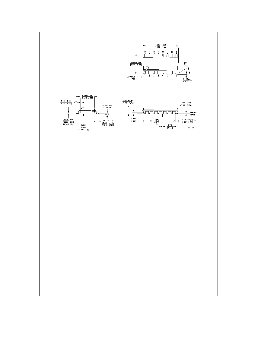
Physical Dimensions
inches (millimeters)
16-Lead Small Outline Molded Package (M)
Order Number DM74LS353M
NS Package Number M16A
5