TL F 9830
DM74LS375
4-Bit
Latch
February 1992
DM74LS375
4-Bit Latch
General Description
The 'LS375 is a 4-bit D-type latch for use as temporary stor-
age for binary information between processing units and in-
put output or indicator units When its Enable (E) input is
HIGH a latch is transparent i e the Q output will follow the
D input each time it changes When E is LOW a latch stores
the last valid data present on the D input preceding the
HIGH-to-LOW transition of E The 'LS375 is functionally
identical to the 'LS75 except for the corner power pins
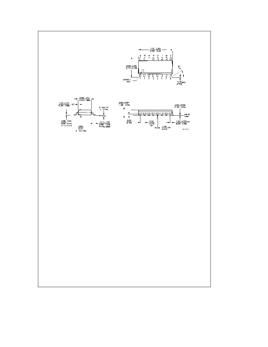
Connection Diagram
Dual-In-Line Package
TL F 9830 ≠ 1
Logic Symbol
TL F 9830 ≠ 2
V
CC
e
Pin 16
GND
e
Pin 8
Order Number DM74LS375M or DM74LS375N
See NS Package Number M16A or N16E
Pin Name
Description
D1 ≠ D4
Data Inputs
E1 2
Latches 1 2 Enable Inputs
E3 4
Latches 3 4 Enable Inputs
Q1 ≠ Q4
Latch Outputs
Q1 ≠ Q4
Complementary Latch Outputs
C1995 National Semiconductor Corporation
RRD-B30M115 Printed in U S A

Absolute Maximum Ratings
(Note)
Supply Voltage
7V
Input Voltage
7V
Operating Free Air Temperature Range
0 C to
a
70 C
Storage Temperature Range
b
65 C to
a
150 C
Note
The ``Absolute Maximum Ratings are those values
beyond which the safety of the device cannot be guaran-
teed The device should not be operated at these limits The
parametric values defined in the ``Electrical Characteristics''
table are not guaranteed at the absolute maximum ratings
The ``Recommended Operating Conditions'' table will define
the conditions for actual device operation
Recommended Operating Conditions
Symbol
Parameter
Min
Nom
Max
Units
V
CC
Supply Voltage
4 75
5
5 25
V
V
IH
High Level Input Voltage
2
V
V
IL
Low Level Input Voltage
0 8
V
I
OH
High Level Output Current
b
0 4
mA
I
OL
Low Level Output Current
8
mA
T
A
Free Air Operating Temperature
0
70
C
t
s
(H)
Setup Time HIGH or LOW
20
ns
t
s
(L)
D
n
to E
n
t
h
(H)
Hold Time HIGH or LOW
0
ns
t
h
(L)
D
n
to E
n
t
w
(H)
E
n
Pulse Width HIGH
20
ns
Electrical Characteristics
Over recommended operating free air temperature range (unless otherwise noted)
Symbol
Parameter
Conditions
Min
Typ
Max
Units
(Note 1)
V
I
Input Clamp Voltage
V
CC
e
Min I
I
e b
18 mA
b
1 5
V
V
OH
High Level Output
V
CC
e
Min I
OH
e
Max
2 7
3 4
V
Voltage
V
IL
e
Max
V
OL
Low Level Output
V
CC
e
Min I
OL
e
Max
0 35
0 5
Voltage
V
IH
e
Min
V
I
OL
e
4 mA V
CC
e
Min
0 25
0 4
I
I
Input Current
Max
V
CC
e
Max V
I
e
7V
Others
0 1
mA
Input Voltage
Enable Input
0 4
mA
I
IH
High Level Input Current
V
CC
e
Max V
I
e
2 7V
Others
20
m
A
Enable Input
80
m
A
I
IL
Low Level Input Current
V
CC
e
Max V
I
e
0 4V
Others
b
0 4
mA
Enable Input
b
1 2
mA
I
OS
Short Circuit Output Current
V
CC
e
Max (Note 2)
b
20
b
100
mA
I
CC
Supply Current
V
CC
e
Max
12
mA
Note 1
All typicals are at V
CC
e
5V T
A
e
25 C
Note 2
Not more than one output should be shorted at a time and the duration should not exceed one second
2

Switching Characteristics
V
CC
e a
5 0V T
A
e a
25 C
Symbol
Parameter
C
L
e
15 pF
Units
Min
Max
t
PLH
Propagation Delay
27
ns
t
PHL
D
n
to Q
n
23
t
PLH
Propagation Delay
20
ns
t
PHL
D
n
to Q
n
15
t
PLH
Propagation Delay
27
ns
t
PHL
E
n
to Q
n
25
t
PLH
Propagation Delay
30
ns
t
PHL
E
n
to Q
n
18
Truth Table
(Each Latch)
t
n
t
n a 1
D
Q
H
H
L
L
t
n
e
Bit time before Enable negative going transition
t
n
a
1
e
Bit time after Enable negative going transition
H
e
HIGH Voltage Level
L
e
LOW Voltage Level
Logic Diagram
(1 4 of diagram shown)
TL F 9830 ≠ 3
3