 | ÐлекÑÑоннÑй компоненÑ: DP8307A | СкаÑаÑÑ:  PDF PDF  ZIP ZIP |
Äîêóìåíòàöèÿ è îïèñàíèÿ www.docs.chipfind.ru
TL F 8794
DP8307A
8-Bit
TRI-STATE
Bidirectional
Transceiver
(Inverting)
February 1996
DP8307A 8-Bit TRI-STATE
Bidirectional Transceiver (Inverting)
General Description
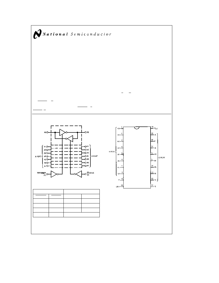
The DP8307A is a high speed Schottky 8-bit TRI-STATE
bidirectional transceiver designed to provide bidirectional
drive for bus oriented microprocessor and digital communi-
cations systems It is capable of sinking 16 mA on the A
ports and 48 mA on the B ports (bus ports) PNP inputs for
low input current and an increased output high (V
OH
) level
allow compatibility with MOS CMOS and other technolo-
gies that have a higher threshold and less drive capabilities
In addition it features glitch-free power up down on the B
port preventing erroneous glitches on the system bus in
power up or down
DP8303A and DP7304B DP8304B are featured with Trans-
mit Receive (T R) and Chip Disable (CD) inputs to simplify
control logic For greater design flexibility DP8307A and
DP7308 DP8308
is
featured
with
Transmit
(T)
and
Receive (R) control inputs
Features
Y
8-bit bidirectional data flow reduces system package
count
Y
Bidirectional TRI-STATE inputs outputs interface with
bus oriented systems
Y
PNP inputs reduce input loading
Y
Output high votlage interfaces with TTL
MOS
and
CMOS
Y
48 mA 300 pF bus drive capability
Y
Pinouts simplify system interconnections
Y
Independent T and R controls for versatility
Y
Compact 20-pin dual-in-line package
Y
Bus port glitch free power up down
Logic and Connection Diagrams
TL F 8794 1
Logic Table
Control Inputs
Resulting Conditions
Transmit
Receive
A Port
B Port
1
0
OUT
IN
0
1
IN
OUT
1
1
TRI-STATE
TRI-STATE
0
0
Both Active
This is not an intended logic condition and may cause oscillations
Dual-In-Line Package
TL F 8794 2
Top View
Order Number DP8307AN
See NS Package Number N20A
TRI-STATE
is a registered trademark of National Semiconductor Corporation
C1996 National Semiconductor Corporation
RRD-B30M36 Printed in U S A
http
www national com
Absolute Maximum Ratings
(Note 1)
If Military Aerospace specified devices are required
please contact the National Semiconductor Sales
Office Distributors for availability and specifications
Supply Voltage
7V
Input Voltage
5 5V
Output Voltage
5 5V
Maximum Power Dissipation at 25 C
Cavity Package
1667 mW
Molded Package
1832 mW
Derate cavity package 11 1 mW C above 25 C derate molded package
14 7 mW C above 25 C
Lead Temperature (soldering 4 sec )
260 C
Storage Temperature
b
65 C to
a
150 C
Recommended Operating
Conditions
Min
Max
Units
Supply Voltage (V
CC
)
4 75
5 25
V
Temperature (T
A
)
0
70
C
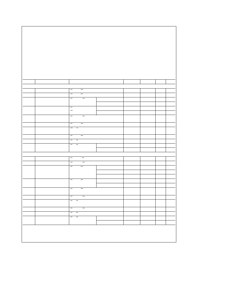
DC Electrical Characteristics
(Notes 2 and 3)
Symbol
Parameter
Conditions
Min
Typ
Max
Units
A PORT (A0 A7)
V
IH
Logical ``1'' Input Voltage
T
e
V
IL
R
e
2 0V
2 0
V
V
IL
Logical ``0'' Input Voltage
T
e
V
IL
R
e
2 0V
0 7
V
V
OH
Logical ``1'' Output Voltage
T
e
2 0V R
e
V
IL
I
OH
e b
0 4 mA
V
CC
b
1 15
V
CC
b
0 7
V
V
IL
e
0 5V
I
OH
e b
3 mA
2 7
3 95
V
V
OL
Logical ``0'' Output Voltage
T
e
2 0V
I
OL
e
16 mA
0 35
0 5
V
R
e
V
IL
I
OL
e
8 mA
0 3
0 4
V
I
OS
Output Short Circuit
T
e
2 0V R
e
V
IL
V
O
e
0V
b
10
b
38
b
75
mA
Current
V
CC
e
Max (Note 4)
I
IH
Logical ``1'' Input Current
T
e
V
IL
R
e
2 0V V
IH
e
2 7V
0 1
80
m
A
I
I
Input Current at Maximum
R
e
T
e
2 0V V
CC
e
Max V
IH
e
5 25V
1
mA
Input Voltage
I
IL
Logical ``0'' Input Current
T
e
V
IL
R
e
2 0V V
IN
e
0 4V
b
70
b
200
m
A
V
CLAMP
Input Clamp Voltage
T
e
R
e
2 0V I
IN
e b
12 mA
b
0 7
b
1 5
V
I
OD
Output Input
T
e
R
e
2 0V
V
IN
e
0 4V
b
200
m
A
TRI-STATE Current
V
IN
e
4 0V
80
m
A
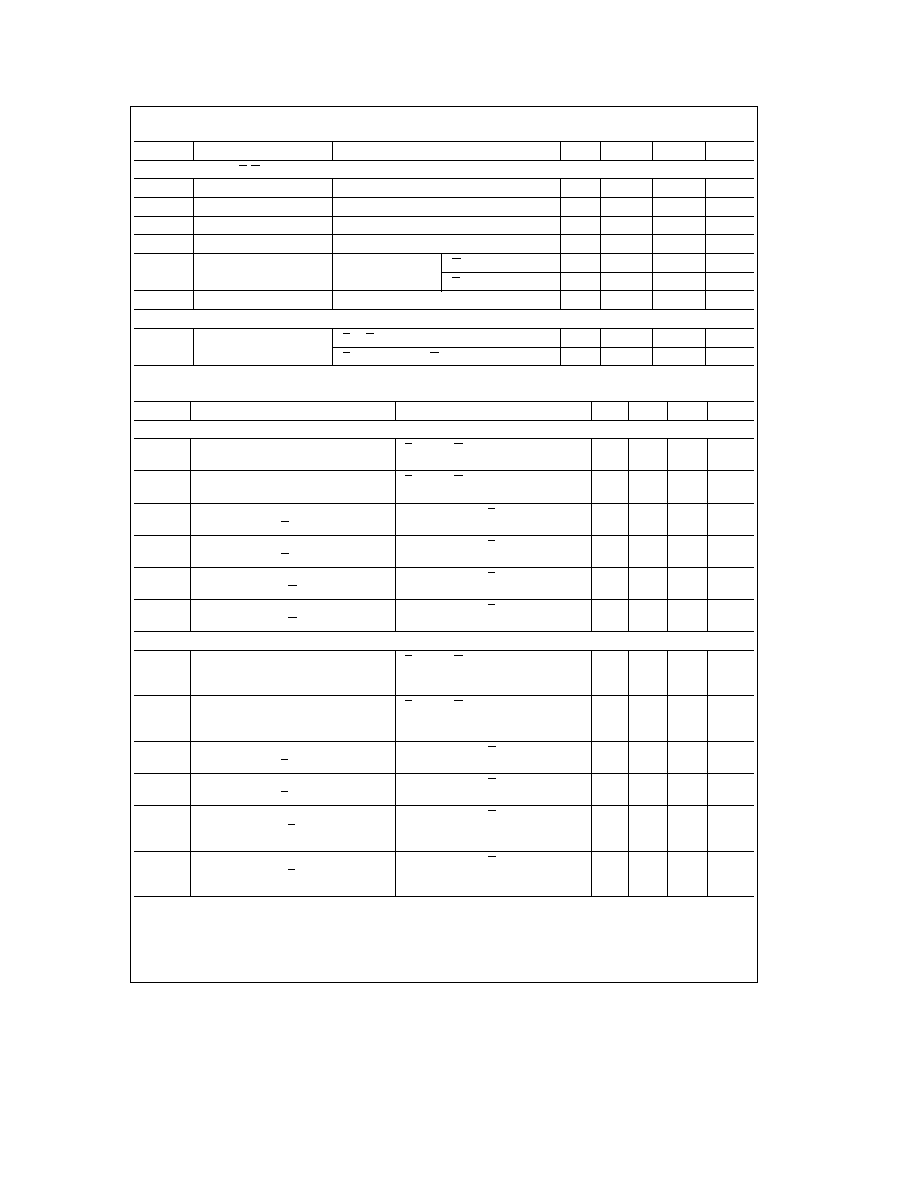
B PORT (B0 B7)
V
IH
Logical ``1'' Input Voltage
T
e
2 0V R
e
V
IL
2 0
V
V
IL
Logical ``0'' Input Voltage
T
e
2 0V R
e
V
IL
0 7
V
V
OH
Logical ``1'' Output Voltage
T
e
V
IL
R
e
2 0V
I
OH
e b
0 4 mA
V
CC
b
1 15
V
CC
b
0 8
V
V
IL
e
0 5V
I
OH
e b
5 mA
2 7
3 9
V
I
OH
e b
10 mA
2 4
3 6
V
V
OL
Logical ``0'' Output Voltage
T
e
V
IL
R
e
2 0V
I
OL
e
20 mA
0 3
0 4
V
I
OL
e
48 mA
0 4
0 5
V
I
OS
Output Short Circuit
T
e
V
IL
R
e
2 0V V
O
e
0V
b
25
b
50
b
150
mA
Current
V
CC
e
Max (Note 4)
I
IH
Logical ``1'' Input Current
T
e
2 0V R
e
V
IL
V
IH
e
2 7V
0 1
80
m
A
I
I
Input Current at Maximum
T
e
R
e
2 0V V
CC
e
Max V
IH
e
5 25V
1
mA
Input Voltage
I
IL
Logical ``0'' Input Current
T
e
2 0V R
e
V
IL
V
IN
e
0 4V
b
70
b
200
m
A
V
CLAMP
Input Clamp Voltage
T
e
R
e
2 0V I
IN
e b
12 mA
b
0 7
b
1 5
V
I
OD
Output Input
T
e
R
e
2 0V
V
IN
e
0 4V
b
200
m
A
TRI-STATE Current
V
IN
e
4 0V
a
200
m
A
http
www national com
2
DC Electrical Characteristics
(Notes 2 and 3) (Continued)
Symbol
Parameter
Conditions
Min
Typ
Max
Units
CONTROL INPUTS T R
V
IH
Logical ``1'' Input Voltage
2 0
V
V
IL
Logical ``0'' Input Voltage
0 7
V
I
IH
Logical ``1'' Input Current
V
IH
e
2 7V
0 5
20
m
A
I
I
Maximum Input Current
V
CC
e
Max V
IH
e
5 25V
1 0
mA
I
IL
Logical ``0'' Input Current
V
IL
e
0 4V
R
b
0 1
b
0 25
mA
T
b
0 25
b
0 5
mA
V
CLAMP
Input Clamp Voltage
I
IN
e b
12 mA
b
0 8
b
1 5
V
POWER SUPPLY CURRENT
I
CC
Power Supply Current
T
e
R
e
2 0V V
IN
e
2 0V V
CC
e
Max
70
100
mA
T
e
0 4V V
INA
e
R
e
2V V
CC
e
Max
100
150
mA
AC Electrical Characteristics
V
CC
e
5V T
A
e
25 C
Symbol
Parameter
Conditions
Min
Typ
Max
Units
A PORT DATA MODE SPECIFICATIONS
t
PDHLA
Propagation Delay to a Logical ``0'' from
T
e
2 4V R
e
0 4V
(Figure A)
8
12
ns
B Port to A Port
R1
e
1k R2
e
5k C1
e
30 pF
t
PDLHA
Propagation Delay to a Logical ``1'' from
T
e
2 4V R
e
0 4V
(Figure A)
11
16
ns
B Port to A Port
R1
e
1k R2
e
5k C1
e
30 pF
t
PLZA
Propagation Delay from a Logical ``0'' to
B0 to B7
e
2 4V T
e
2 4V
(Figure B)
10
15
ns
TRI-STATE from R to A Port
S3
e
1 R5
e
1k C4
e
15 pF
t
PHZA
Propagation Delay from a Logical ``1'' to
B0 to B7
e
0 4V T
e
2 4V
(Figure B)
8
15
ns
TRI-STATE from R to A Port
S3
e
0 R5
e
1k C4
e
15 pF
t
PZLA
Propagation Delay from TRI-STATE to
B0 to B7
e
2 4V T
e
2 4V
(Figure B)
25
35
ns
a Logical ``0'' from R to A Port
S3
e
1 R5
e
1k C4
e
30 pF
t
PZHA
Propagation Delay from TRI-STATE to
B0 to B7
e
0 4V T
e
2 4V
(Figure B)
24
35
ns
a Logical ``1'' from R to A Port
S3
e
0 R5
e
5k C4
e
30 pF
B PORT DATA MODE SPECIFICATIONS
t
PDHLB
Propagation Delay to a Logical ``0'' from
T
e
0 4V R
e
2 4V
(Figure A)
A Port to B Port
R1
e
100X R2
e
1k C1
e
300 pF
12
18
ns
R1
e
667X R2
e
5k C1
e
45 pF
8
12
ns
t
PDLHB
Propagation Delay to a Logical ``1'' from
T
e
0 4V R
e
2 4V
(Figure A)
A Port to B Port
R1
e
100X R2
e
1k C1
e
300 pF
15
23
ns
R1
e
667X R2
e
5k C1
e
45 pF
9
14
ns
t
PLZB
Propagation Delay from a Logical ``0'' to
A0 to A7
e
2 4V R
e
2 4V
(Figure B)
13
18
ns
TRI-STATE from T to B Port
S3
e
1 R5
e
1k C4
e
15 pF
t
PHZB
Propagation Delay from a Logical ``1'' to
A0 to A7
e
0 4V R
e
2 4V
(Figure B)
8
15
ns
TRI-STATE from T to B Port
S3
e
0 R5
e
1k C4
e
15 pF
t
PZLB
Propagation Delay from TRI-STATE to
A0 to A7
e
2 4V R
e
2 4V
(Figure B)
a Logical ``0'' from T to B Port
S3
e
1 R5
e
100X C4
e
300 pF
32
40
ns
S3
e
1 R5
e
667X C4
e
45 pF
18
25
ns
t
PZHB
Propagation Delay from TRI-STATE to
A0 to A7
e
0 4V R
e
2 4V (
Figure B )
a Logical ``1'' from T to B Port
S3
e
0 R5
e
1k C4
e
300 pF
25
35
ns
S3
e
0 R5
e
5k C4
e
45 pF
16
25
ns
Note 1
``Absolute Maximum Ratings'' are those values beyond which the safety of the device cannot be guaranteed They are not meant to imply that the devices
should be operated at these limits The tables of ``Electrical Characteristics'' provide conditions for actual device operation
Note 2
Unless otherwise specified min max limits apply across the supply and temperature range listed in the table of Recommended Operating Conditions All
typical values given are for V
CC
e
5V and T
A
e
25 C
Note 3
All currents into device pins are positive all currents out of device pins are negative All voltages are referenced to ground unless otherwise specified
Note 4
Only one output at a time should be shorted
http
www national com
3
Switching Time Waveforms and AC Test Circuits
TL F 8794 3
TL F 8794 4
Note
C1 includes test fixture capacitance
FIGURE A Propagation Delay from A Port to B Port or from B Port to A Port
TL F 8794 5
TL F 8794 6
Note
C4 includes test fixture capacitance Port input is in a fixed logical condition See AC Table
FIGURE B Propagation Delay to from TRI-STATE from R to A Port and T to B Port
http
www national com
4

http
www national com
5