
TL F 9365
DP83910A
CMOS
SNI
Serial
Network
Interface
May 1995
DP83910A CMOS SNI
Serial Network Interface
General Description
The DP83910A CMOS Serial Network Interface (SNI) is a
direct-pin equivalent of the bipolar DP8391 SNI and pro-
vides the Manchester data encoding and decoding func-
tions for IEEE 802 3 Ethernet Thin-Ethernet type local area
networks The SNI interfaces the DP8390 Network Interface
Controller (NIC) to the DP8392 CTI or an Ethernet transceiv-
er cable When transmitting the SNI converts non-return-to-
zero (NRZ) data from the controller into Manchester data
and sends the converted data differentially to the transceiv-
er Conversely when receiving a Phase Lock Loop de-
codes the 10 Mbit s data from the transceiver into NRZ
data for the controller
The DP83910A operates in conjunction with the DP8392
Coaxial Transceiver Interface (CTI) and the DP8390 Net-
work Interface Controller (NIC) to form a three-chip set that
implements a complete IEEE 802 3 compatible network as
shown below The DP83910A is a functionally complete
Manchester encoder decoder including a balanced driver
and receiver on-board crystal oscillator collision signal
translator
and
a
diagnostic
loopback
feature
The
DP83910A fabricated CMOS typically consumes less than
70 mA of current However as a result of being CMOS the
DP83910A's differential signals must be isolated in both
Ethernet and thin wire Ethernet
Features
Y
Compatible with Ethernet I
IEEE 802 3
10BASE5
10BASE2 and 10BASE-T
Y
Designed to interface with 10BASE-T transceivers
Y
Functional and pin-out duplicate of the DP8391
Y
10 Mbits s Manchester encoding decoding with receive
clock recovery
Y
Requires no precision components
Y
Loopback capability for diagnostics
Y
Externally selectable half or full step modes of opera-
tion at transmit output
Y
Squelch circuitry at the receive and collision inputs to
reject noise
Y
TTL MOS compatible controller interface
1 0 System Diagram
IEEE 802 3 Compatible Ethernet Thin-Ethernet 10 BaseT
Local Area Network Chip Set
TL F 9365 � 1
TRI-STATE
is a registered trademark of National Semiconductor Corporation
C1995 National Semiconductor Corporation
RRD-B30M105 Printed in U S A
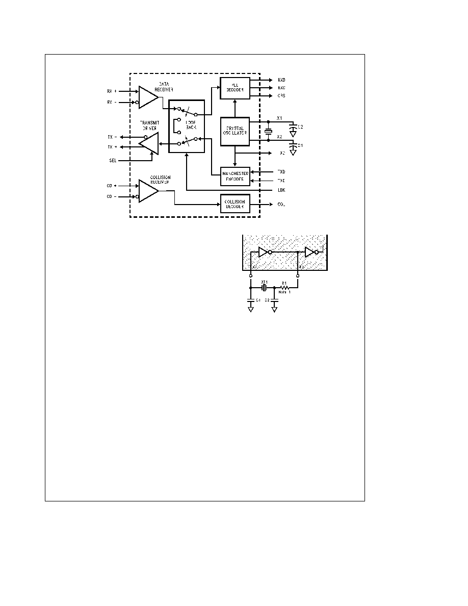
2 0 Block Diagram
TL F 9365 � 2
3 0 Functional Description
The DP83910A consists of five main logical blocks
a) The oscillator generates the 10 MHz transmit clock signal
for system timing
b) The Manchester encoder accepts NRZ data from the
controller encodes the data to Manchester and trans-
mits it differentially to the transceiver through the differ-
ential transmit driver
c) The Manchester decoder receives Manchester data from
the transceiver converts it to NRZ data and clock pulses
and sends it to the controller
d) The collision translator indicates to the controller the
presence of a valid 10 MHz collision signal to the PLL
e) The loopback circuitry when asserted routes the data
from the Manchester encoder back to the PLL decoder
3 1 OSCILLATOR
The oscillator is controlled by a 20 MHz parallel resonant
crystal connected between X1 and X2 or by an external
clock on X1 The 20 MHz output of the oscillator is divided
by 2 to generate the 10 MHz transmit clock for the control-
ler The oscillator also provides internal clock signals to the
encoding and decoding circuits
If a crystal is connected to the DP83910A it is recommend-
ed that the circuit shown in
Figure 1 be used and that the
components used meet the following
Crystal XT1 AT cut parallel resonant crystal
Series Resistance
s
10X
Specified Load Capacitance 13 5 pF
Accuracy 0 005% (50 ppm)
C1 C2 Load Capacitor 27 pF
The resistor R1 in
Figure 1 may be required in order to
minimize frequency drift due to changes in the V
CC
supply
voltage If R1 is required it's value must be carefully select-
ed R1 decreases the loop gain Thus if R1 is made too
large the loop gain will be greatly reduced and the crystal
will not oscillate If R1 is made too small normal variations
in the V
CC
may cause the oscillation frequency to drift out of
specification As the first rule of thumb the value of R1
TL F 9365 � 15
Note 1
The resistor R1 may be required in order to minimize frequency drift
due to changes in the V
CC
See text description
FIGURE 1 Crystal Connection to DP83910A
(see text for component values)
should be made equal to five times the motional resistance
of the crystal
The motional resistance of 20 MHz crystals is usually in the
range of 10X to 30X This implies that a reasonable value
for R1 should be in the range of 50X � 150X
The decision of whether or not to include R1 should be
based upon measured variations of crystal frequency as
each of the circuit parameters is varied
According to the IEEE 802 3 standard the entire oscillator
circuit (crytsal and amplifier) must be accurate to 0 01%
When using a crystal the X1 pin is not guaranteed to pro-
vide a TTL compatible logic output and should not be used
to drive external standard logic If additional logic needs to
be driven then an external oscillator should be used as
described in the following
3 2 OSCILLATOR MODULE OPERATION
If the designer wishes to use a crystal clock oscillator one
that provides the following should be employed
1) TTL or CMOS output with a 0 01% frequency tolerance
2) 40% � 60% duty cycle
3)
t
2 TTL load output drive (I
OL
e
3 2 mA)
2

3 0 Functional Description
(Continued)
The circuit is shown in
Figure 2 (Additional output drive may
be necessary if the oscillator must also drive other compo-
nents ) When using a clock oscillator it is still recommended
that the designer connect the oscillator output to the X1 pin
and tie the X2 pin to ground
3 3 MANCHESTER ENCODER AND
DIFFERENTIAL DRIVER
The encoder begins operation when the Transmit Enable
input (TXE) goes high and converts clock and NRZ data to
Manchester data for the transceiver For the duration of
TXE remaining high the Transmitted Data (TXD) is encoded
for the transmit-driver pair (TX
g
) TXD must be valid on the
rising edge of Transmit Clock (TXC) Transmission ends
when TXE goes low The last transition is always positive it
occurs at the center of the bit cell if the last bit is a one or at
the end of the bit cell if the last bit is a zero
The differential transmit pair from the secondary of the iso-
lation transformer drives up to 50 meters of twisted pair AUI
cable These outputs are source followers which require two
270X pull-down resistors to ground
The DP83910A allows both half-step and full-step to be
compatible with Ethernet I and IEEE 802 3 With the SEL pin
low (for Ethernet I) transmit
a
is positive with respect to
transmit
b
during idle with SEL high (for IEEE 802 3)
transmit
a
and transmit
b
are equal in the idle state This
provides zero differential voltage to operate with transform-
er coupled loads
TL F 9365 � 16
FIGURE 2 DP83910A Connection for Oscillator Module
3 4 MANCHESTER DECODER
The decoder consists of a differential receiver and a PLL to
separate Manchester encoded data stream into clock sig-
nals and NRZ data The differential input must be externally
terminated with two 39X resistors connected in series if the
standard 78X transceiver drop cable is used in Thin-Ether-
net applications these resistors are optional To prevent
noise from falsely triggering the decoder a squelch circuit at
the input rejects signals with levels less than
b
175 mV
Once the input exceeds the squelch requirements Carrier
Sense (CRS) is asserted Receive data (RXD) and receive
clock (RXC) become valid typically within 6 bit times The
DP83910A may tolerate bit jitter up to 18 ns in the received
data
The decoder detects the end of a frame when no more
midbit transitions are detected Within one and a half bit
times after the last bit carrier sense is de-asserted Receive
clock stays active for five more bit times after CRS goes low
to guarantee the receive timings of the DP8390 NIC
3 5 COLLISION TRANSLATOR
When the Ethernet transceiver (DP8392 CTI) detects a colli-
sion it generates a 10 MHz signal to the differential collision
inputs (CD
g
) of the DP83910A When these inputs are de-
tected active the DP83910A translates the 10 MHz signal
to an active high level for the controller The controller uses
this signal to back off its current transmission and resched-
ule another one
The collision differential inputs are terminated the same way
as the differential receive inputs The squelch circuitry is
also similar rejecting pulses with levels less than
b
175 mV
3 6 LOOPBACK FUNCTIONS
When the Loopback input (LBK) is asserted high the
DP83910A redirects its transmitted data back into its re-
ceive path This feature provides a convenient method for
testing both chip and system level integrity The transmit
driver and receive input circuitry are disabled in loopback
mode
4 0 Connection Diagrams
TL F 9365 � 17
Top View
Order Number DP83910AV
See NS Package Number V28A
TL F 9365 � 18
Top View
Order Number DP83910AN
See NS Package Number N24C
3

5 0 Typical Application
Interface
for
Ethernet
and
Thin
Wire
Ethernet
Using
Single
Jumper
for
ThinThick
Selection
TLF9365
�
3
4

6 0 Pin Descriptions
24-Pin DIP
28-Pin PCC
Name
I O
Description
1
1
COL
O
COLLISION DETECT OUTPUT
Generates an active high signal when
10 MHz collision signal is detected
2
2
RXD
O
RECEIVE DATA OUTPUT
NRZ data output from the PLL This signal
must be sampled on the rising edge of receive clock
3
3
CRS
O
CARRIER SENSE
Asserted on the first valid high-to-low transition on
the RX
g
pair Remains active until 1 5 bit times after the last bit in
data
4
4
RXC
O
RECEIVE CLOCK
The receive clock from the Manchester data after
the PLL has locked Remains active 5 bit times after deasserting CRS
5
5
SEL
I
MODE SELECT
When high transmit
a
and transmit
b
are the same
voltage in the idle state When low transmit
a
is positive with respect
to transmit
b
in the idle state at the transformer's primary
6
7
V
SS
GROUND PIN
8
V
SS
9
V
SS
7
10
LBK
I
LOOPBACK
When high the loopback mode is enabled
8
11
X1
I
CRYSTAL OR EXTERNAL OSCILLATOR INPUT
9
12
X2
O
CRYSTAL FEEDBACK OUTPUT
Used in crystal connections only
Connected to ground when using an external oscillator
10
13
TXD
I
TRANSMIT DATA INPUT
NRZ data input from the controller The
data is combined with the transmit clock to produce Manchester data
TXD is sampled on the rising edge of transmit clock
11
14
TXC
O
TRANSMIT CLOCK
The 10 MHz clock derived from the 20 MHz
oscillator
12
15
TXE
I
TRANSMIT ENABLE
The encoder begins operation when this input is
asserted high
13
16
TX
b
O
TRANSMIT OUTPUT
Differential line driver which sends the encoded
data to the transceiver The outputs are source followers which require
14
17
TX
a
270X pull-down resistors
15
6
NC
NO CONNECTION
This may be tied to V
SS
for the PLCC version to be
compatible with the DP8391
16
18
NC
NO CONNECTION
17
19
TEST
I
FACTORY TEST INPUT
Used to check the chip's internal functions
May be tied low or have a 0 01 mf bypass capacitor to ground (for
compatibility with the bipolar DP8391) during normal operation
18
20
V
DD
POWER CONNECTION
19
21
V
DD
22
V
DD
23
V
DD
20
24
NC
NO CONNECTION
21
25
RX
b
I
RECEIVE INPUT
Differential receive input pair from the transceiver
22
26
RX
a
23
27
CD
b
I
COLLISION INPUT
Differential collision pair input from the
transceiver
24
28
CD
a
5