 | –≠–ª–µ–∫—Ç—Ä–æ–Ω–Ω—ã–π –∫–æ–º–ø–æ–Ω–µ–Ω—Ç: DP84902MS | –°–∫–∞—á–∞—Ç—å:  PDF PDF  ZIP ZIP |

TL F 11963
DP84902
17
EncoderDecoder
Circuit
June 1994
DP84902
1 7 Encoder Decoder Circuit
General Description
The DP84902 is designed to perform the encoding and de-
coding for disk memory systems It is designed to interface
directly with Integrated Read Channel Products (such as
National Semiconductor's DP84910) and with Disk Data
Controller Products with a 2-bit NRZ interface (such as Na-
tional Semiconductor's Advanced Disk Controllers) This
Encoder Decoder (ENDEC) circuit employs a 2 3 (1 7) Run
Length Limited (RLL) code type and supports the hard sec-
tored format
The DP84902 has the option of selecting either TTL or ECL
compatible code output to interface with preamplifiers com-
monly used in high data rate applications This is accomm-
plished by the setting of a bit in the control register
The ENDEC also includes write data precompensation con-
trol circuitry which detects the need for write precompensa-
tion This circuitry issues early and late output signals nec-
essary for precompensation The precompensation informa-
tion is generated against a 2T pattern The precompensa-
tion circuitry can be bypassed by the setting of a bit in the
control register
A control reigster is included to configure the ENDEC and to
select device operation options such as output code inver-
sion differential code output bypassing of the encoder and
the use of an internal write clock
The DP84902 is available in 20-pin SO and 20-pin SSO
packages
Features
Y
Operates at 2-bit Non-Return to Zero (NRZ) Data Rates
up to 50 Mbits second
Y
Single
a
5V Power Supply Operation
Y
Low Power Dissipation when TTL compatible code out-
put is selected 150 mW at 50 Mbits second NRZ Rate
Y
TTL Compatible Inputs and Outputs
Y
ECL Compatible Code Outputs (patented) are control
register selectable
Y
Two-bit NRZ Interface
Y
Supports Write Data Precompensation with Early and
Late output signals
Y
Selectable use of either an Internal or External Write
Clock
Y
Power Down Mode Included
Y
DC-Erasure is available to support Analog Flaw Map-
ping Testing
Y
Bypass Mode available which permits Un-Encoded Test
Patterns to be issued at the CODEOUT Pin
Block Diagram
TL F 11963 ≠ 1
FIGURE 1 DP84902 ENDEC Block Diagram
TRI-STATE
is a registered trademark of National Semiconductor Corporation
IBM
is a registered trademark of International Business Machines Corporation
C1995 National Semiconductor Corporation
RRD-B30M105 Printed in U S A
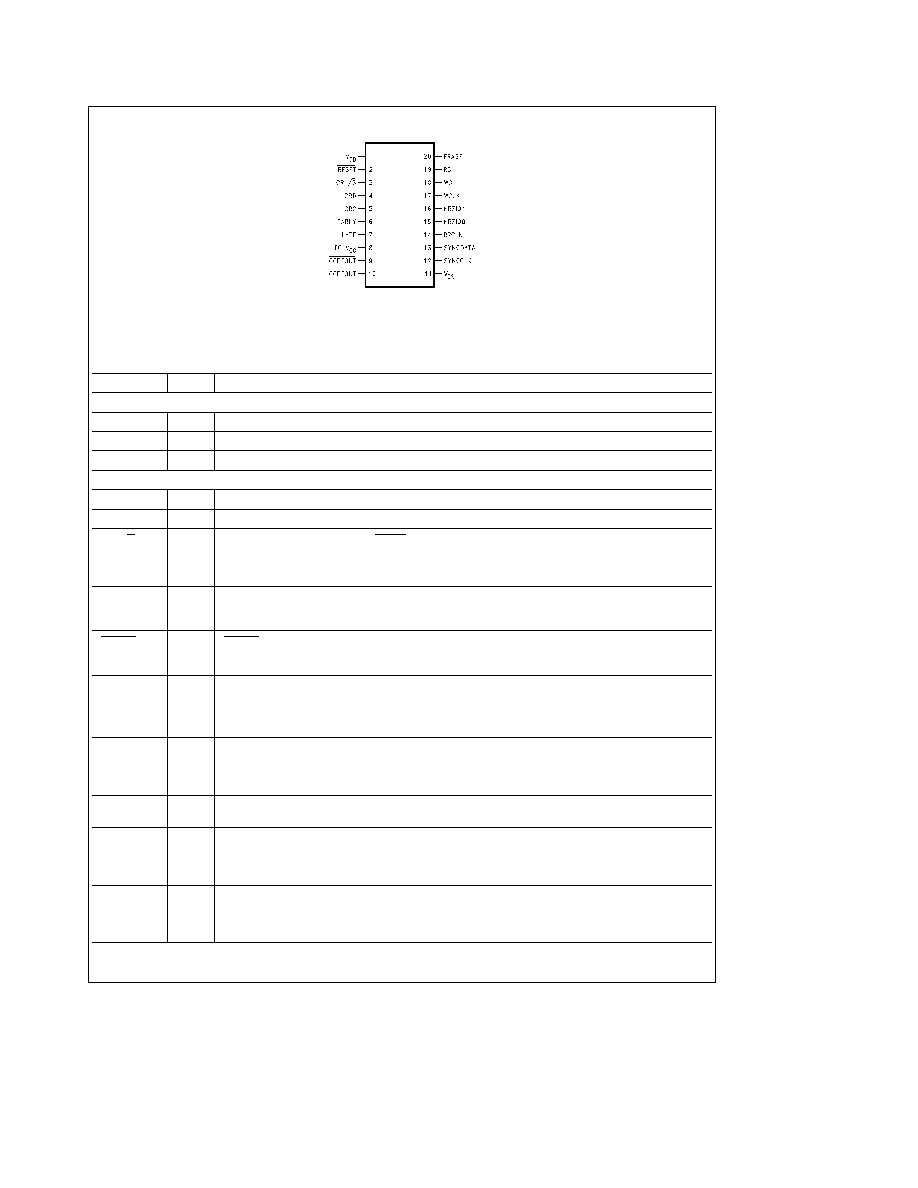
Connection Diagram
TL F 11963 ≠ 2
FIGURE 2 DP84902 Pinout
Order Number DP84902M or DP84902MS
See NS Package Number M20B or MSA20
Pin Descriptions
Symbol
Pin
Functional Description
Power Supply and Ground Pins
ECLV
CC
8
ECLV
CC
Supply Pin 5V
g
10%
V
DD
1
V
DD
Supply Pin 5V
g
10%
V
SS
11
V
SS
Ground reference
Input Pin Descriptions
CRC
5
CONTROL REGISTER CLOCK
Positive-edge-active control register clock input
CRD
4
CONTROL REGISTER DATA
Control register data input
CRL S
3
CONTROL REGISTER LATCH SHIFT
A logical low state applied to this input allows the CONTROL
REGISTER CLOCK input to clock data into the control register's shift register via the CONTROL
REGISTER DATA input A logical high state latches the data into a bank of latches and issues the
information to the appropriate circuitry within the ENDEC
ERASE
20
ERASE
This active high input is used while in the write mode to force a logical low at the CODEOUT
output (or a logical high if CODEOUT is inverted) This is useful to blank out (DC erase which issues no
transitions) a track for analog flaw map tesing
RESET
2
RESET
A logical low level applied to this input forces the ENDEC to a power-on-reset state and
presets its control register to predetermined operating setup conditions During normal operation this
pin must be held at a logical high level
RG
19
READ GATE
This input accepts a mode control signal from the controller for the decoder It permits
the reading of data from the disk when at a logical high level It inhibits reading and resets the decoder
state machine when at a logical low level There are no set-up or hold timing requirements for the
enabling or disabling of this input
SYNCCLK
12
SYNCHRONIZED CLOCK
This input accepts the code rate (1 5F) synchronized clock signal from the
read channel's data synchronizer This signal is used to clock the synchronized data into the decoder
on the negative edge of SYNCCLK in the read mode and is the source clock for clocking codeout data
from the encoder during the write mode
SYNCDATA
13
SYNCHRONIZED DATA
This input accepts the synchronized data signal MSB first from the read
channel's data synchronizer for the decoder's use
WCLK
17
WRITE CLOCK
This input is used only in the external write clock mode The write clock signal (Note 1)
from the controller is used to strobe the NRZ input data into the ENDEC The write clock signal from the
controller must be the RRCLK echoed by the controller If the external write clock mode is not selected
this pin should be tied to V
DD
or V
SS
WG
18
WRITE GATE
This input accepts a mode control signal from the controller for the encoder It permits
the writing of a header and data to the disk when at a logical high level It inhibits writing and resets the
encoder state machine when at a logical low level There are no set-up or hold timing requirements for
the enabling or disabling of this input
2

Pin Descriptions
(Continued)
Symbol
Pin
Functional Description
Output Pin Descriptions
CODEOUT
10
(1 7) RLL CODE OUTPUT
This output issues encoded data MSB first to be written to the disk The
control register controls various attributes of this output It can be configured either as a TTL or ECL
compatible output In the TTL mode the sense of the output can be selectively inverted to allow the
active edge to be either the positive or negative transition and can also be put into a high impedance
state (TRI-STATE ) which allows the multiplexing of this pin with another device or pin The
precompensation circuitry can be bypassed The encoder can also be bypassed thus permitting uncoded
test patterns to be issued from this pin
CODEOUT
9
(1 7) RLL COMPLEMENTARY CODE OUTPUT
This output is the complement of the ECL differential
CODEOUT output pin It issues encoded data to be written to the disk It is enabled as an ECL output by
a control register bit If the TTL mode is selected (by a control register bit) this pin will be in a high
impedance state (TRI-STATE)
EARLY
6
EARLY PRECOMPENSATION OUTPUT
This pin is the early precompensation output It issues a logical
high level to indicate that early precompensation is needed This signal is used by National
Semiconductor Integrated Read Channel Products such as the DP8492 to precompensate the final
coded data before it goes to the read write circuit
LATE
7
LATE PRECOMPENSATION OUTPUT
This pin is the late precompensation output It issues a logical
high level to indicate that late precompensation is needed This signal is used by National
Semiconductor Integrated Read Channel Products such as the DP8492 to precompensate the final
coded data before it goes to the read write circuit
RRCLK
14
READ REFERENCE CLOCK
This output issues read clock to the controller at all times (Note 1) This
signal is used to clock decoded NRZ data into the controller in the read mode (READ CLOCK) and is to
be echoed back to the ENDEC by the controller in the write mode for use as a write clock (REFERENCE
CLOCK) if external write clock mode is selected in the control register
Input Output Pin Descriptions
NRZIO0
15
LEAST SIGNIFICANT BIT NRZ INPUT OUTPUT
This I O pin represents the Least Significant Bit
(LSB) of NRZ data As an input it accepts the NRZ LSB data signal from the controller Data is strobed
into the ENDEC on the positive-edge of the WRITE CLOCK (if external write clock mode is selected in
the control register) encoded and written to the disk in (1 7) format This NRZ input must be low while
the preamble and address mark fields are being written This pin is also used to transfer un-encoded test
patterns to the CODEOUT pin As an output it issues the decoded NRZ LSB data to the controller during
a read operation NRZ output data will be clocked into the controller on the positive-edge of the READ
REFERENCE CLOCK (RRCLK)
NRZIO1
16
MOST SIGNIFICANT BIT NRZ INPUT OUTPUT
This I O pin represents the Most Significant Bit (MSB)
of NRZ data As an input it accepts the NRZ MSB data signal from the controller Data is strobed into
the ENDEC on the positive-edge of the WRITE CLOCK (if external write clock mode is selected in the
control register) encoded and written to the disk in (1 7) format This NRZ input must be held low while
the preamble and address mark fields are being written As an output this pin issues the decoded NRZ
MSB data to the controller during a read operation The decoded NRZ output data will be clocked into
the controller on the positive-edge of the READ REFERENCE CLOCK (RRCLK)
Note 1
With the code rate at 1 5F the effective NRZ data rate is 1F Since this chip employs a 2-bit NRZ interface the write (WCLK) and read reference (RRCLK)
clocks are 0 5F
3
DC and AC Device Specifications
Absolute Maximum Ratings
(Note)
Note
Absolute Maximum Ratings are those values beyond which the safety
of the device cannot be guaranteed The device should not be oper-
ated at these limits The parametric values defined in the ``Electrical
Characteristics'' tables are not guaranteed at these ratings The ``op-
erating conditions'' table will define the conditions for actual device
operation
Supply Voltage
7V
TTL Input Maximum Voltage
7V
Maximum Output Voltage
7V
ESD Susceptibility (Note 1)
2000V
Note 1
Human Body model used (100 pF through 1 5 kX)
General Operating Conditions
are guaranteed over supply voltage and operating ambient temperature
ranges unless otherwise specified
Symbol
Parameter
Min
Typ
Max
Units
Test
(Note 1)
V
DD
ECLV
CC
Supply Voltage
4 5
5
5 5
V
N A
T
A
Operation Ambient Temperature
0
70
C
N A
T
S
Storage Temperature
b
65
150
C
N A
C
LOAD
Capacitive Load on any Output
ECL Output
10
pF
N A
TTL Output
15
I
OH
High Logic Level Output Current
b
8
mA
(Note A)
(CMOS Logic Outputs Only)
I
OL
Low Logic Level Output Current
EARLY LATE
6
mA
(Note A)
(CMOS Logic Outputs Only)
All Others
8
(Note A)
V
IH
High Logic Level Input Voltage
2
V
(Note A)
V
IL
Low Logic Level Input Voltage
0 8
V
(Note A)
f
NRZ
NRZ Transfer Rate Operating Frequency
5
50
Mb s
(Note A)
f
SCLK
SYNCCLK Operating Frequency
7 5
75
MHz
(Note A)
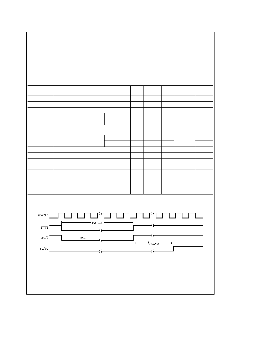
t
PW(RESET)
RESET Pulse Width (negative)
5
SYNCCLK
(Note A)
(See
Figure 3 )
PERIODS
t
PW(RG WG)
RG or WG Wait Time after Power Down or Reset
SYNCCLK
with Respect to Positive Edge of CRL S Pin
10
PERIODS
(Note B)
(See
Figure 3 )
Note 1
Typical values are specified at 25 C and 5V supply
Note A
This parameter is guaranteed by outgoing testing
Note B
The limit values have been determined by characterization data No outgoing tests are performed
TL F 11963 ≠ 3
Note
Power down mode selected in control register (see Table I)
FIGURE 3 Reset Pin and Power Down Timing Diagram
4

Control Register Operating Conditions
are guaranteed over operating conditions (see table) unless
otherwise specified
Symbol
Parameter
Min
Typ
Max
Units
Test
(Note 1)
t
PW(CRC)
CRC Pulse Width (positive or negative) (see
Figures 4 and 9 )
14
ns
(Note A)
t
SU(CRD)
CRD Setup Time with respect to CRC (positive edge)
5
ns
(Note A)
(see
Figures 4 and 8 )
t
H(CRD)
CRD Hold Time with respect to CRC (positive edge)
5
ns
(Note A)
(see
Figures 4 and 8 )
t
SU(CRL S)
CRL S Setup Time with respect to CRC (positive edge)
5
ns
(Note A)
(see
Figures 4 and 8 )
t
H(CRL S)
CRL S Hold Time with respect to CRC (positive edge)
5
ns
(Note A)
(see
Figures 4 and 8 )
Note 1
Typical values are specified at 25 C and 5V supply
Note A
This parameter is guaranteed by outgoing testing
TL F 11963 ≠ 4
FIGURE 4 Control Register Timing Diagram
5