Äîêóìåíòàöèÿ è îïèñàíèÿ www.docs.chipfind.ru
TL F 5852
DS0025C
Two
Phase
MOS
Clock
Driver
June 1992
DS0025C Two Phase MOS Clock Driver
General Description
The DS0025C is a monolithic low cost two phase MOS
clock driver that is designed to be driven by TTL line drivers
or buffers such as the DS8830 or DM7440 Two input cou-
pling capacitors are used to perform the level shift from TTL
to MOS logic levels Optimum performance in turn-off delay
and fall time are obtained when the output pulse is logically
controlled by the input However output pulse width may be
set by selection of the input capacitor eliminating the need
for tight input pulse control
Features
Y
8-lead TO-5 or 8-lead or 14-lead dual-in-line package
Y
High Output Voltage Swings
up to 25V
Y
High Output Current Drive Capability
up to 1 5A
Y
Rep Rate 1 0 MHz into
l
1000 pF
Y
Driven by DS8830 DM7440
Y
``Zero'' Quiescent Power
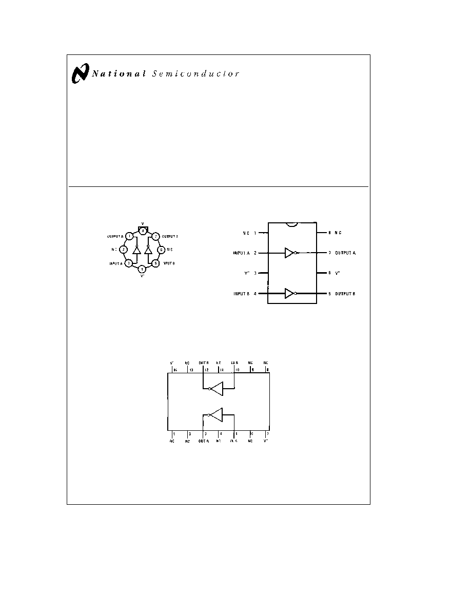
Connection Diagrams
Metal Can Package
TL F 5852 1
Note Pin 4 connected to case
Top View
Order Number DS0025CH
See NS Package Number H08C
Dual-In-Line Package
TL F 5852 2
Top View
Order Number DS0025CJ-8
or DS0025CN
See NS Package Number J08A or N08E
Dual-In-Line Package
TL F 5852 3
Top View
Order Number DS0025CJ
See NS Package Number J14A
C1995 National Semiconductor Corporation
RRD-B30M105 Printed in U S A
Absolute Maximum Ratings
(Note 1)
If Military Aerospace specified devices are required
please contact the National Semiconductor Sales
Office Distributors for availability and specifications
(V
a
b
V
b
)Voltage Differential
25V
Input Current
100 mA
Peak Output Current
1 5A
Storage Temperature
b
65 C to
a
150 C
Operating Temperature
0 C to
a
85 C
Lead Temperature (Soldering 10 sec)
300 C
Recommended Operating
Conditions
V
a
V
b
Differential Voltage
20V
Min
Max
Temperature
0
70
Maximum Power Dissipation at 25 C
8-Pin Cavity Package
1150 mW
14-Pin Cavity Package
1410 mW
Molded Package
1080 mW
Metal Can (TO-5) Package
670 mW
Derate 8-pin cavity package 7 8 mW C above 25 C de-
rate 14-pin cavity package 9 5 mW C above 25 C derate
molded package 8 7 mW C above 25 C derate metal
can (TO-5) package 4 5 mW C above 25 C
Electrical Characteristics
(Notes 2 and 3) See test circuit
Symbol
Parameter
Conditions
Min
Typ
Max
Units
t
d ON
Turn-On Delay Time
C
IN
e
0 001 mF R
IN
e
0X C
L
e
0 001 mF
15
30
ns
t
RISE
Rise Time
C
IN
e
0 001 mF R
IN
e
0X C
L
e
0 001 mF
25
50
ns
t
d OFF
Turn-Off Delay Time
C
IN
e
0 001 mF R
IN
e
0X C
L
e
0 001 mF
30
60
ns
(Note 4)
t
FALL
Fall Time
C
IN
e
0 001 mF R
IN
e
0X
(Note 4)
60
90
120
ns
C
L
e
0 001 mF
(Note 5)
100
150
250
ns
PW
Pulse Width (50% to 50%)
C
IN
e
0 001 mF R
IN
e
0X
500
ns
C
L
e
0 001 mF (Note 5)
V
Oa
Positive Output Voltage Swing
V
IN
e
0V I
OUT
e b
1 mA
V
a
b
1 0
V
a
b
0 7V
V
V
Ob
Negative Output Voltage Swing
I
IN
e
10 mA I
OUT
e
1 mA
V
b
a
0 7V
V
b
a
1 5V
V
Note 1
``Absolute Maximum Ratings'' are those values beyond which the safety of the device cannot be guaranteed Except for ``Operating Temperature Range''
they are not meant to imply that the devices should be operated at these limits The table of ``Electrical Characteristics'' provides conditions for actual device
operation
Note 2
Unless otherwise specified min max limits apply across the 0 C to 70 C range for the DS0025C
Note 3
All currents into device pins shown as positive out of device pins as negative all voltages referenced to ground unless otherwise noted All values shown
as max or min on absolute value basis
Note 4
Parameter values apply for clock pulse width determined by input pulse width
Note 5
Parameter values for input width greater than output clock pulse width
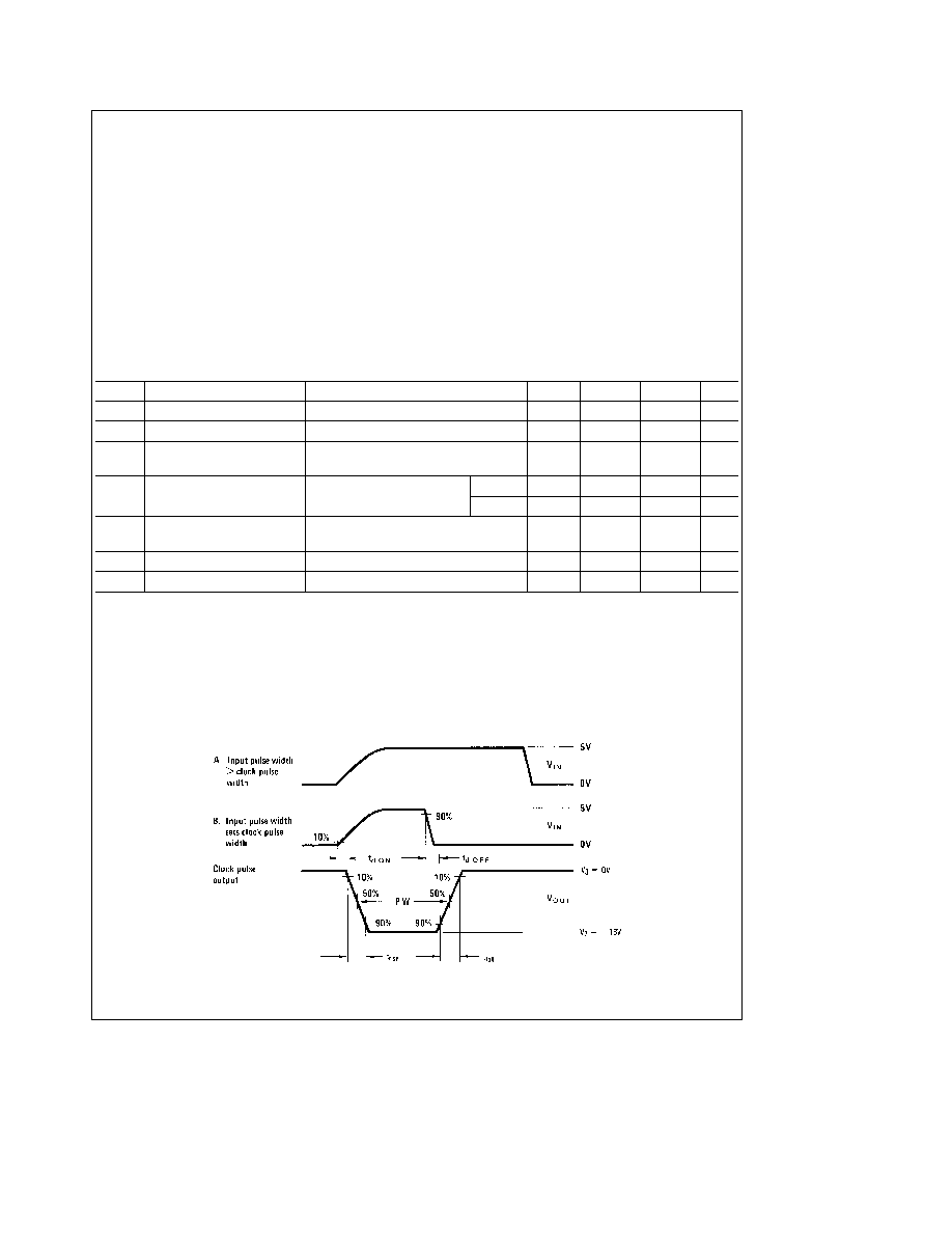
Timing Diagram
Input waveform
PRR
e
0 5 MHz
V
P-P
e
5 0V
t
r
e
t
f
s
10 ns
Pulse width
A 1 0 ms
B 200 ns
TL F 5852 5
2
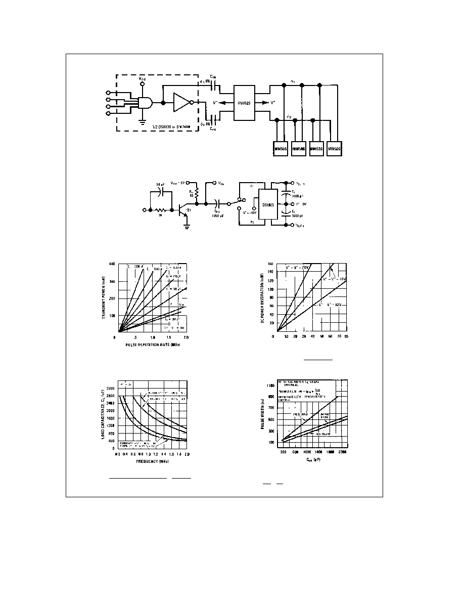
Typical Application
TL F 5852 4
AC Test Circuit
TL F 5852 6
Q1 is selected high speed NPN switching transistor
Typical Performance
Transient Power vs Rep Rate
TL F 5852 7
P
AC
e
(V
a
V
b
)
2
fC
L
DC Power (P
DC
) vs Duty Cycle
TL F 5852 8
DUTY CYCLE (%)
P
DC
e
V
a
V
b
)
2
(DC)
1k
Maximum Load Capacitance
TL F 5852 9
C
L
k
(P
MAX
) (1k)(V
a
b
V
b
)
2
(DC)
(f) (1k) (V
a
b
V
b
)
2
k
(I
pk
) (t
r
)
V
a
b
V
b
Output PW Controlled by C
IN
TL F 5852 10
I
MAX
e
Peak Current delivered by driver
I
MIN
V
BE
R1
e
0 6
1k
3
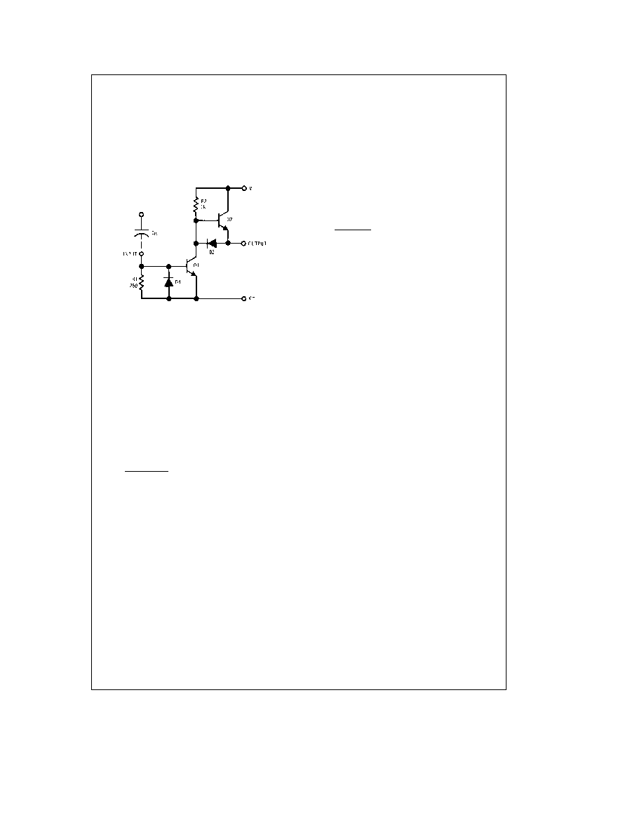
Applications Information
Circuit Operation
Input current forced into the base of Q
1
through the cou-
pling capacitor C
IN
causes Q
1
to be driven into saturation
swinging the output to V
b
a
V
CE
(sat)
a
V
Diode
When the input current has decayed or has been switched
such that Q
1
turns off Q
2
receives base drive through R
2
turning Q
2
on This supplies current to the load and the
output swings positive to V
a
V
BE
TL F 5852 11
FIGURE 1 DS0025 Schematic (One-Half Circuit)
It may be noted that Q
1
must switch off before Q
2
begins to
supply current hence high internal transients currents from
V
b
to V
a
cannot occur
Fan-Out Calculation
The drive capability of the DS0025 is a function of system
requirements
i e
speed
ambient temperature
voltage
swing drive circuitry and stray wiring capacity
The following equations cover the necessary calculations to
enable the fan-out to be calculated for any system condi-
tion
Transient Current
The maximum peak output current of the DS0025 is given
as 1 5A Average transient current required from the driver
can be calculated from
I
e
C
L
(V
a
V
b
)
t
r
(1)
Typical rise times into 1000 pF load is 25 ns For V
a
b
V
b
e
20V I
e
0 8A
Transient Output Power
The average transient power (P
ac
) dissipated is equal to
the energy needed to charge and discharge the output ca-
pacitive load (C
L
) multiplied by the frequency of operation
(f)
P
AC
e
C
L
x (V
a
V
b
)
2
x f
(2)
For V
a
b
V
b
e
20V f
e
1 0 MHz C
L
e
1000 pF P
AC
e
400 mW
Internal Power
``0'' State
Negligible (
k
3 mW)
``1'' State
P
int
e
(V
a
V
b
)
2
R
2
x Duty Cycle
(3)
e
80 mW for V
a
V
b
e
20V DC
e
20%
Package Power Dissipation
Total average power
e
transient output power
a
internal
power
Example Calculation
How many MM506 shift registers can be driven by a
DS0025CN driver at 1 MHz using a clock pulse width of 200
ns rise time 30 50 ns and 16V amplitude over the tempera-
ture range 0 70 C
Power Dissipation
At 70 C the DS0025CN can dissipate 870 mW when sol-
dered into printed circuit board
Transient Peak Current Limitation
From equation (1) it can be seen that at 16V and 30 ns the
maximum load that can be driven is limited to 2800 pF
Average Internal Power
Equation (3) gives an average power of 50 mW at 16V and
a 20% duty cycle
For one-half of the DS0025C 870 mW
d
2 can be dissipat-
ed
435 mW
e
50 mW
a
transient output power
385 mW
e
transient output power
Using equation (2) at 16V 1 MHz and 350 mW each half of
the DS0025CN can drive a 1367 pF load This is less than
the load imposed by the transient current limitation of equa-
tion (1) and so a maximum load of 1367 pF would prevail
From the data sheet for the MM506 the average clock
pulse load is 80 pF Therefore the number of devices driven
is 1367 80 or 17 registers
For further information please refer to National Semicon-
ductors Application Note AN-76
4
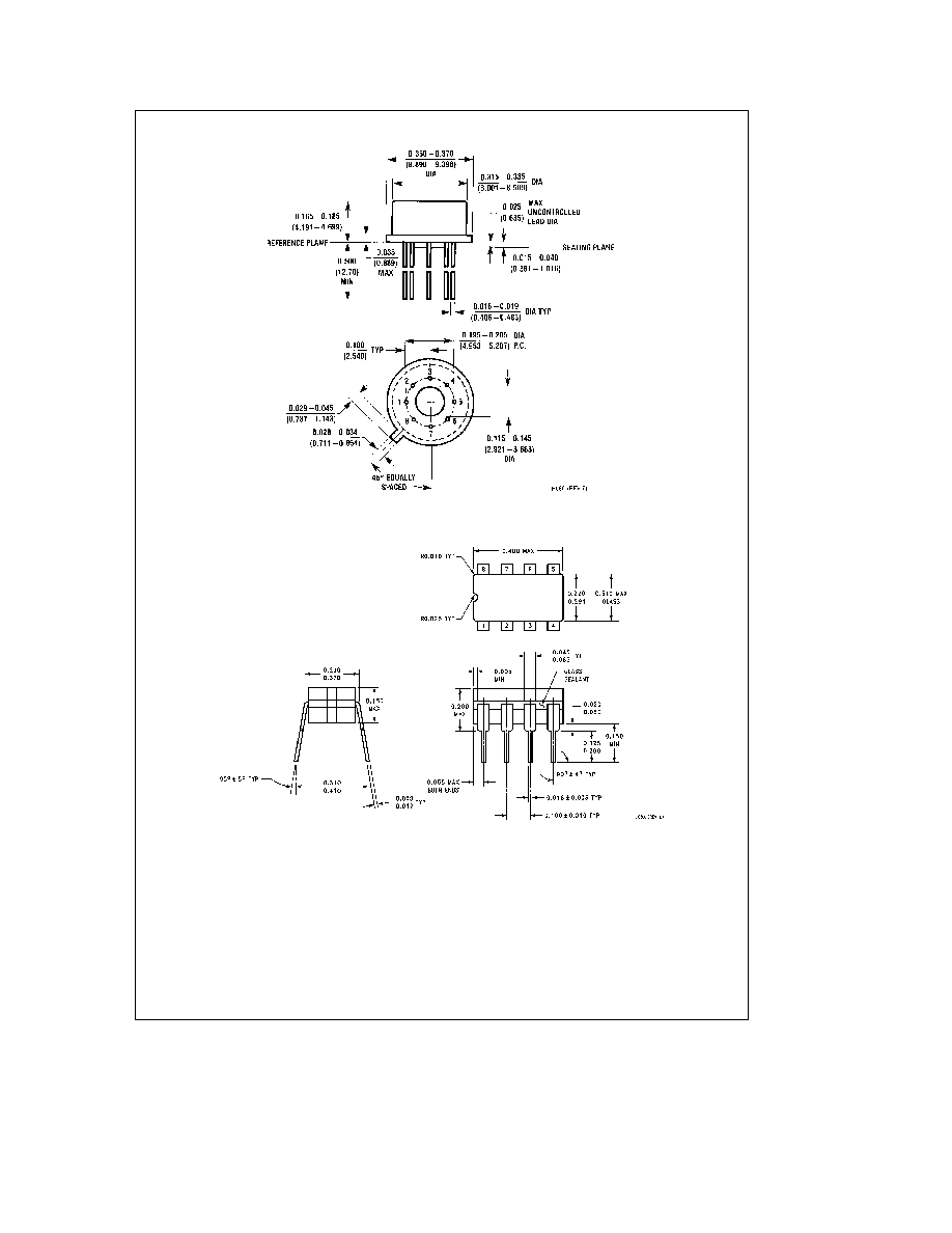
Physical Dimensions
inches (millimeters)
Order Number DS0025CH
NS Package Number H08C
Order Number DS0025CJ
NS Package Number J08A
5