 | ÐлекÑÑоннÑй компоненÑ: DS0026C | СкаÑаÑÑ:  PDF PDF  ZIP ZIP |
DS0026 Dual High-Speed MOS Driver
DS0026
Dual High-Speed MOS Driver
General Description
DS0026 is a low cost monolithic high speed two phase MOS
clock driver and interface circuit. Unique circuit design pro-
vides both very high speed operation and the ability to drive
large capacitive loads. The device accepts standard TTL
outputs and converts them to MOS logic levels. The device
may be driven from standard 54/74 series and 54S/74S
series gates and flip-flops or from drivers such as the
DS8830 or DM7440. The DS0026 is intended for applica-
tions in which the output pulse width is logically controlled;
i.e., the output pulse width is equal to the input pulse width.
The DS0026 is designed to fulfill a wide variety of MOS
interface requirements. Information on the correct usage of
the DS0026 in these as well as other systems is included in
the application note AN-76.
Features
n
Fast rise and fall times -- 20 ns 1000 pF load
n
High output swing -- 20V
n
High output current drive --
±
1.5 amps
n
TTL compatible inputs
n
High rep rate -- 5 to 10 MHz depending on power
dissipation
n
Low power consumption in MOS "0" state -- 2 mW
n
Drives to 0.4V of GND for RAM address drive
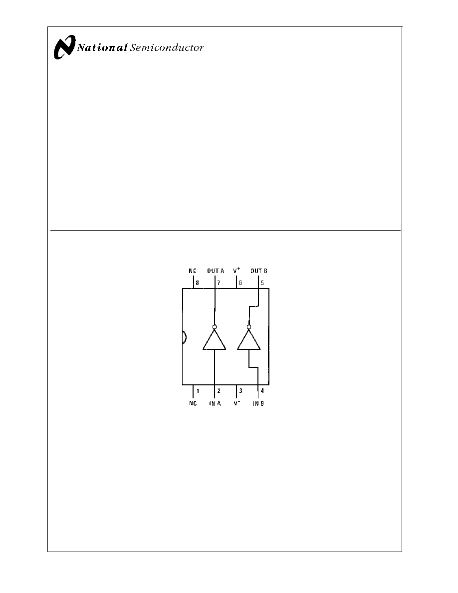
Connection Diagram (Top View)
Dual-In-Line Package
00585302
February 2002
DS0026
Dual
High-Speed
MOS
Driver
© 2002 National Semiconductor Corporation
DS005853
www.national.com
Absolute Maximum Ratings
(Note 1)
If Military/Aerospace specified devices are required,
please contact the National Semiconductor Sales Office/
Distributors for availability and specifications.
(V
+
) - (V
-
) Differential Voltage
22V
Input Current
100 mA
Input Voltage (V
IN
) - (V
-
)
5.5V
Peak Output Current
1.5A
Storage Temperature Range
-65°C to +150°C
Lead Temperature
(Soldering, 10 sec.)
300°C
Operating Ratings
(V
+
) - (V
-
) Differential Voltage
10V to 20V
Maximum Power Dissipation at T
A
= 25°C (Note 7)
1168mW
N08E
JA
107°C/W
N08E
JC
37°C/W
M08A
JA
180°C/W
MUA08A
JA
220°C/W
Operating Temperature Range, T
A
0°C to +70°C
Ordering Information
Order Number
Package Type
NS Package Number
DS0026CN
M-DIP
N08E
DS0026CMA
SOIC
M08A
DS0026CMM
MSOP
MUA08A
Electrical Characteristics
(Notes 2, 3, 4)
Symbol
Parameter
Conditions
Min
Typ
Max
Units
V
IH
Logic "1" Input Voltage
V
-
= 0V
2
1.5
V
I
IH
Logic "1" Input Current
V
IN
- V
-
= 2.4V
10
15
mA
V
IL
Logic "0" Input Voltage
V
-
= 0V
0.6
0.4
V
I
IL
Logic "0" Input Current
V
IN
- V
-
= 0V
-3
-10
µA
V
OL
Logic "1" Output Voltage
V
IN
- V
-
= 2.4V, I
OL
= 1 mA
V
-
+0.7
V
-
+1.0
V
V
OH
Logic "0" Output Voltage
V
IN
- V
-
= 0.4V, V
SS
V
+
+ 1.0V
I
OH
= - 1 mA
V
+
- 1.0
V
+
-0.8
V
I
CC(ON)
"ON" Supply Current
(one side on)
V
+
- V
-
= 20V, V
IN
- V
-
= 2.4V
30
40
mA
I
CC(OFF)
"OFF" Supply Current
V
+
- V
-
= 20V,
V
IN
- V
-
= 0V
10
100
µA
Switching Characteristics
(T
A
= 25°C) (Notes 5, 6)
Symbol
Parameter
Conditions
Min
Typ
Max
Units
t
ON
Turn-On Delay
(Figure 1)
5
7.5
12
ns
(Figure 2)
11
ns
t
OFF
Turn-Off Delay
(Figure 1)
12
15
ns
(Figure 2)
13
ns
t
r
Rise Time
(Figure 1),
(Note 5)
C
L
= 500 pF
15
18
ns
C
L
= 1000 pF
20
35
ns
(Figure 2),
(Note 5)
C
L
= 500 pF
30
40
ns
C
L
= 1000 pF
36
50
ns
t
f
Fall Time
(Figure 1),
(Note 5)
C
L
= 500 pF
12
16
ns
C
L
= 1000 pF
17
25
ns
(Figure 2),
(Note 5)
C
L
= 500 pF
28
35
ns
C
L
= 1000 pF
31
40
ns
Note 1: "Absolute Maximum Ratings" are those values beyond which the safety of the device cannot be guaranteed. Except for "Operating Temperature Range"
they are not meant to imply that the devices should be operated at these limits. The table of "Electrical Characteristics provides conditions for actual device operation.
Note 2: These specifications apply for V
+
- V
-
= 10V to 20V, C
L
= 1000 pF, over the temperature range of 0°C to +70°C for the DS0026CN.
Note 3: All currents into device pins shown as positive, out of device pins as negative, all voltages referenced to ground unless otherwise noted. All values shown
as max or min on absolute value basis.
DS0026
www.national.com
2
Switching Characteristics
(Continued)
Note 4: All typical values for T
A
= 25°C.
Note 5: Rise and fall time are given for MOS logic levels; i.e., rise time is transition from logic "0" to logic "1" which is voltage fall.
Note 6: The high current transient (as high as 1.5A) through the resistance of the internal interconnecting V
-
lead during the output transition from the high state
to the low state can appear as negative feedback to the input. If the external interconnecting lead from the driving circuit to V
-
is electrically long, or has significant
dc resistance, it can subtract from the switching response.
Note 7: Derate N08E package 9.3 mW/°C for T
A
above 25°C.
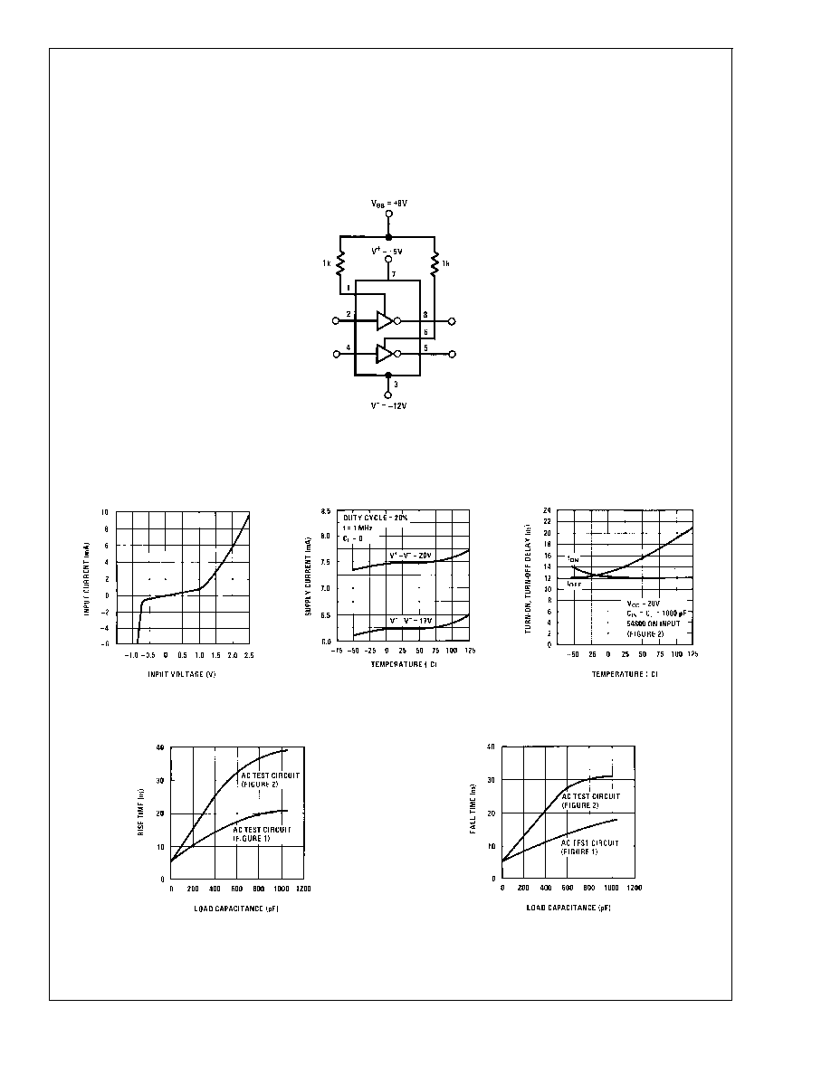
Typical V
BB
Connection
00585308
Typical Performance Characteristics
Input Current vs Input Voltage
Supply Current vs Temperature
Turn-On and Turn-Off Delay
vs Temperature
00585322
00585323
00585324
Rise Time vs Load
Capacitance
Fall Time vs Load
Capacitance
00585325
00585326
DS0026
www.national.com
3
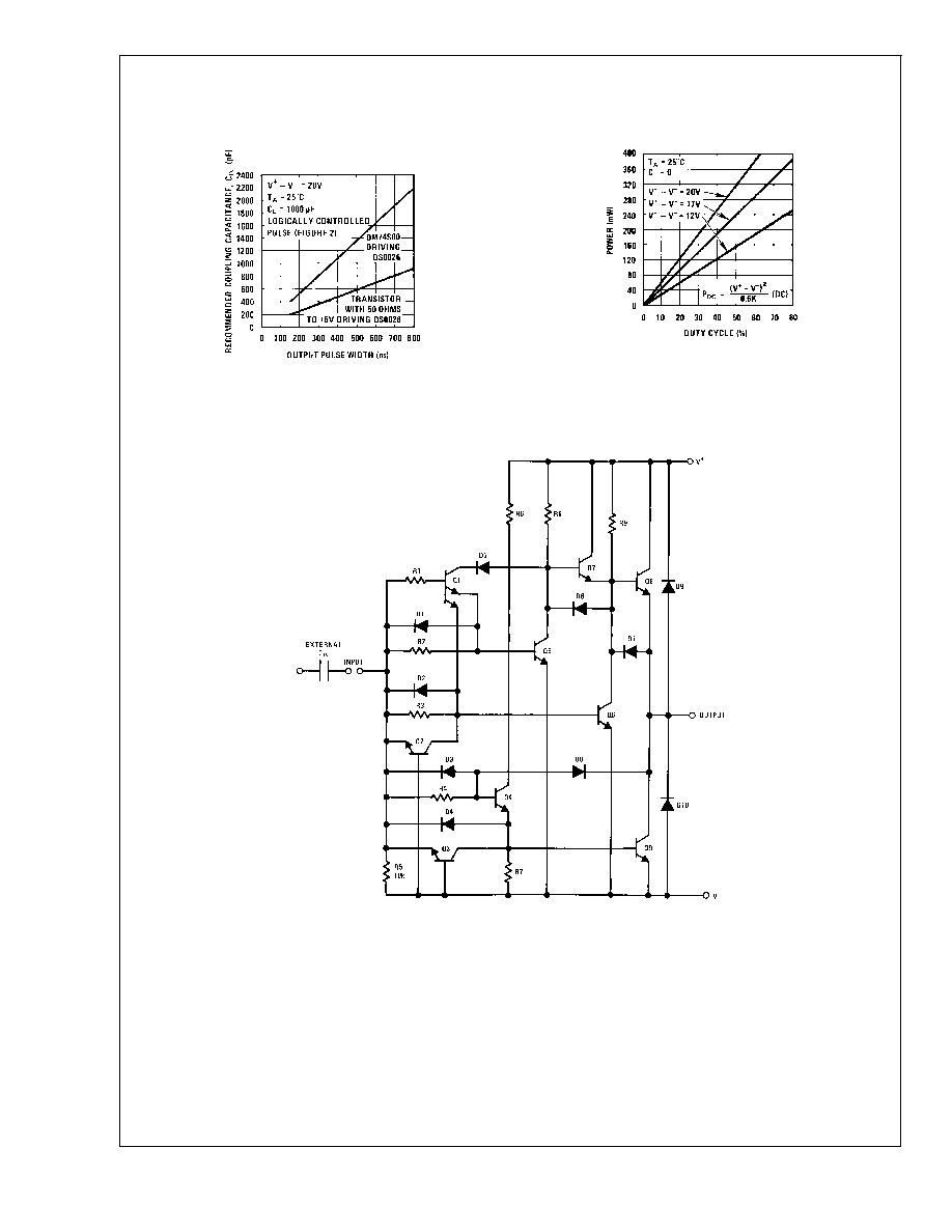
Typical Performance Characteristics
(Continued)
Recommended Input Coding
Capacitance
DC Power (P
DC
) vs
Duty Cycle
00585327
00585328
Schematic Diagram
1/2 DS0026
00585310
DS0026
www.national.com
4
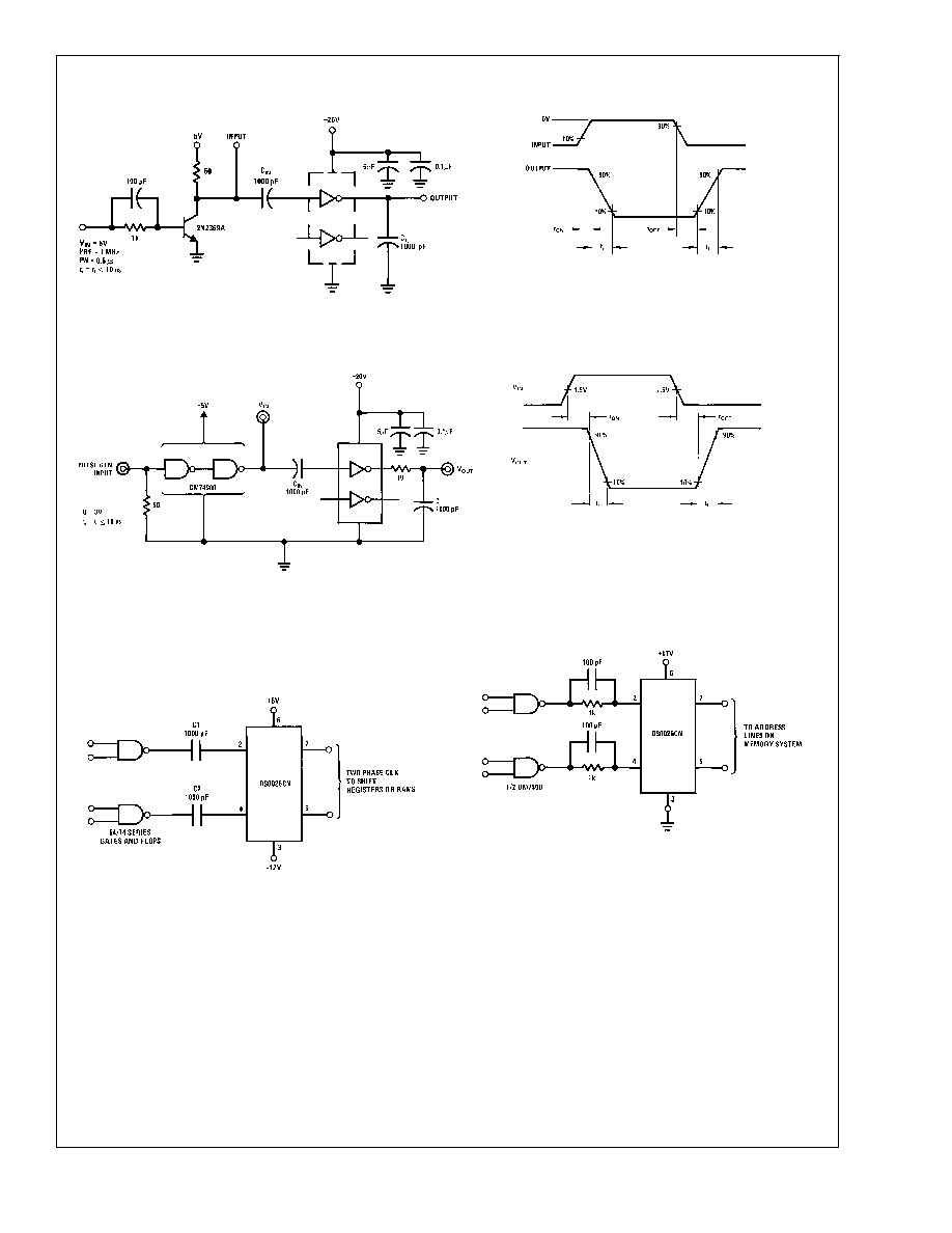
AC Test Circuits and Switching Time Waveforms
Typical Applications
AC Coupled MOS Clock Driver
00585316
DC Coupled RAM Memory Address or Precharge
Driver (Positive Supply Only)
00585317
Application Hints
DRIVING THE MM5262 WITH THE
DS0026 CLOCK DRIVER
The clock signals for the MM5262 have three requirements
which have the potential of generating problems for the user.
These requirements, high speed, large voltage swing and
large capacitive loads, combine to provide ample opportunity
for inductive ringing on clock lines, coupling clock signals to
other clocks and/or inputs and outputs and generating noise
on the power supplies. All of these problems have the po-
tential of causing the memory system to malfunction. Rec-
ognizing the source and potential of these problems early in
the design of a memory system is the most critical step. The
object here is to point out the source of these problems and
give a quantitative feel for their magnitude.
00585312
00585313
FIGURE 1.
00585314
00585315
FIGURE 2.
DS0026
www.national.com
5
Document Outline