 | –≠–ª–µ–∫—Ç—Ä–æ–Ω–Ω—ã–π –∫–æ–º–ø–æ–Ω–µ–Ω—Ç: DS16149 | –°–∫–∞—á–∞—Ç—å:  PDF PDF  ZIP ZIP |
TL F 7553
DS16149DS36149
DS16179DS36179
Hex
MOS
Drivers
February 1986
DS16149 DS36149 DS16179 DS36179 Hex MOS Drivers
General Description
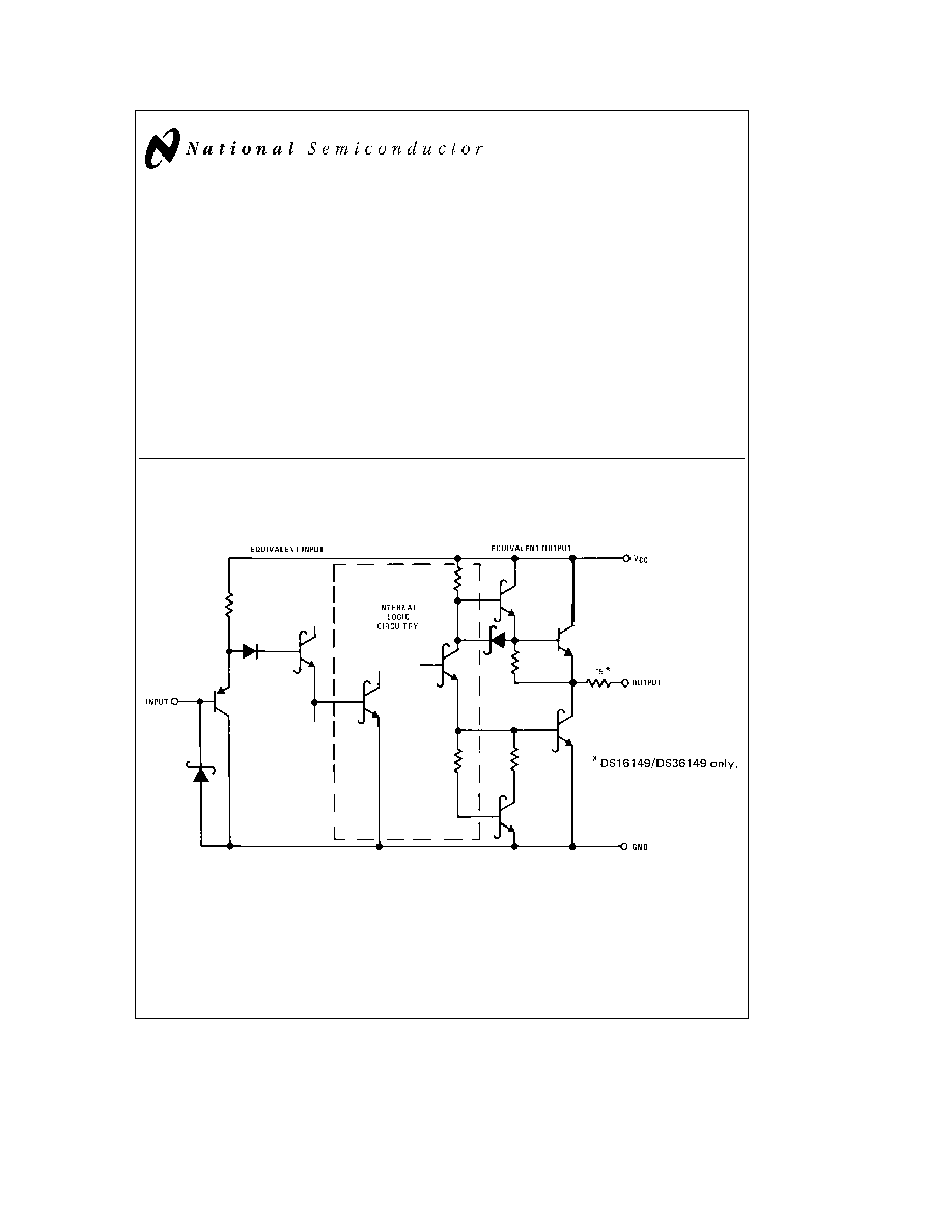
The DS16149 DS36149 and DS16179 DS36179 are Hex
MOS drivers with outputs designed to drive large capacitive
loads up to 500 pF associated with MOS memory systems
PNP input transistors are employed to reduce input currents
allowing the large fan-out to these drivers needed in memo-
ry systems The circuit has Schottky-clamped transistor log-
ic for minimum propagation delay and a disable control that
places the outputs in the logic ``1'' state (see truth table)
This is especially useful in MOS RAM applications where a
set of address lines has to be in the logic `'1'' state during
refresh
The DS16149 DS36149 has a 15 X resistor in series with
the outputs to dampen transients caused by the fast-switch-
ing output The DS16179 DS36179 has a direct low imped-
ance output for use with or without an external resistor
Features
Y
High speed capabilities
Typ 9 ns driving 50 pF
Typ 29 ns driving 500 pF
Y
Built-in 15 X damping resistor (DS16149 DS36149)
Y
Same pin-out as DM8096 and DM74366
Schematic Diagram
TL F 7553 ≠ 1
C1995 National Semiconductor Corporation
RRD-B30M105 Printed in U S A
Absolute Maximum Ratings
(Note 1)
If Military Aerospace specified devices are required
please contact the National Semiconductor Sales
Office Distributors for availability and specifications
Supply Voltage
7 0V
Logical ``1'' Input Voltage
7 0V
Logical ``0'' Input Voltage
b
1 5V
Storage Temperature Range
b
65 C to
a
150 C
Maximum Power Dissipation at 25 C
Cavity Package
1371 mW
Molded Package
1280 mW
Lead Temperature (Soldering 10 seconds)
300 C
Derate cavity package 9 1 mW C above 25 C derate molded package
10 2 m W C above 25 C
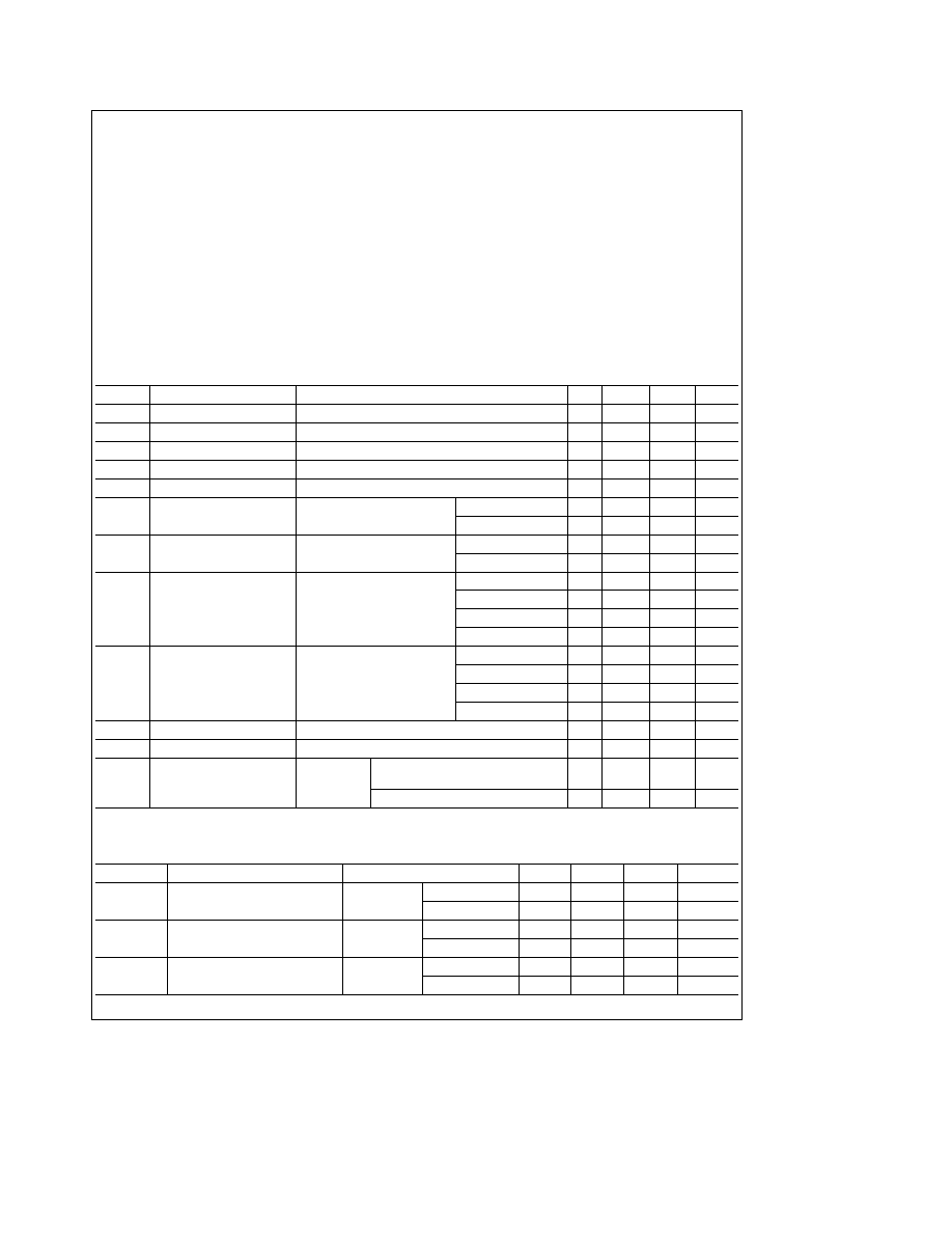
Operating Conditions
Min
Max
Units
Supply Voltage (V
CC
)
4 5
5 5
V
Temperature (T
A
)
DS16149 DS16179
b
55
a
125
C
DS36149 DS36179
0
a
70
C
DC Electrical Characteristics
(Notes 2 and 3)
Symbol
Parameter
Conditions
Min
Typ
Max
Units
V
IN
(1)
Logical ``1'' Input Voltage
2 0
V
V
IN
(0)
Logical ``0'' Input Voltage
0 8
V
I
IN
(1)
Logical ``1'' Input Current
V
CC
e
5 5V V
IN
e
5 5V
0 1
40
m
A
I
IN
(0)
Logical ``0'' Input Current
V
CC
e
5 5V V
IN
e
0 5V
b
50
b
250
m
A
V
CLAMP
Input Clamp Voltage
V
CC
e
4 5V I
IN
e b
18 mA
b
0 75
b
1 2
V
V
OH
Logical ``1'' Output Voltage
V
CC
e
4 5V I
OH
e b
10 mA
DS16149 DS16179
3 4
4 3
V
(No Load)
DS36149 DS36179
3 5
4 3
V
V
OL
Logical ``0'' Output Voltage
V
CC
e
4 5V I
OL
e
10 mA
DS16149 DS16179
0 25
0 4
V
(No Load)
DS36149 DS36179
0 25
0 35
V
V
OH
Logical ``1'' Output Voltage
DS16149
2 4
3 5
V
(With Load)
V
CC
e
4 5V I
OH
e b
1 0 mA
DS16179
2 5
3 5
V
DS36149
2 6
3 5
V
DS36179
2 7
3 5
V
V
OL
Logical ``0'' Output Voltage
DS16149
0 6
1 1
V
(With Load)
V
CC
e
4 5V I
OL
e
20 mA
DS16179
0 4
0 5
V
DS36149
0 6
1 0
V
DS36179
0 4
0 5
V
I
ID
Logical ``1'' Drive Current
V
CC
e
4 5V V
OUT
e
0V (Note 4)
b
250
mA
I
OD
Logical ``0'' Drive Current
V
CC
e
4 5V V
OUT
e
4 5V (Note 4)
150
mA
I
CC
Power Supply Current
Disable Inputs
e
0V
33
60
mA
V
CC
e
5 5V
All Other Inputs
e
3V
All Inputs
e
0V
14
20
mA
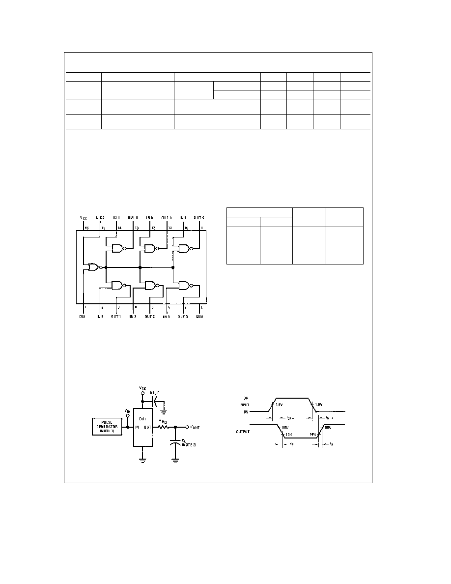
Switching Characteristics
(V
CC
e
5V T
A
e
25 C) (Note 4)
Symbol
Parameter
Conditions
Min
Typ
Max
Units
t
S
g
Storage Delay Negative Edge
(
Figure 1 )
C
L
e
50 pF
4 5
7
ns
C
L
e
500 pF
7 5
12
ns
t
S
'
Storage Delay Positive Edge
(
Figure 1 )
C
L
e
50 pF
5
8
ns
C
L
e
500 pF
8
13
ns
t
F
Fall Time
(
Figure 1 )
C
L
e
50 pF
5
8
ns
C
L
e
500 pF
22
35
ns
2
Switching Characteristics
(V
CC
e
5V T
A
e
25 C) (Note 4) (Continued)
Symbol
Parameter
Conditions
Min
Typ
Max
Units
t
R
Rise Time
(
Figure 1 )
C
L
e
50 pF
6
9
ns
C
L
e
500 pF
26
35
ns
t
LH
Delay from Disable Input
R
L
e
2 kX to Gnd
15
22
ns
to Logical ``1''
C
L
e
50 pF (
Figure 2 )
t
HL
Delay from Disable Input
R
L
e
2 kX to V
CC
11
18
ns
to Logical ``0''
C
L
e
50 pF (
Figure 3 )
Note 1
``Absolute Maximum Ratings'' are those values beyond which the safety of the device cannot be guaranteed Except for ``Operating Temperature Range''
they are not meant to imply that the devices should be operated at these limits The table of ``Electrical Characteristics'' provides conditions for actual device
operation
Note 2
Unless otherwise specified min max limits apply across the
b
55 C to
a
125 C temperature range for the DS16149 and DS16179 and across the 0 C to
a
70 C range for the DS36149 and DS36179 All typical values are for T
A
e
25 C and V
CC
e
5V
Note 3
All currents into device pins shown as positive out of device pins as negative all voltages referenced to ground unless otherwise noted All values shown
as max or min on absolute value basis
Note 4
When measuring output drive current and switching response for the DS16179 and DS36179 a 15 X resistor should be placed in series with each output
This resistor is internal to the DS16149 DS36149 and need not be added
Connection Diagram
Dual In-Line Package
TL F 7553 ≠ 2
Top View
Order Number DS16149J DS36149J DS16179J
DS36179J DS36149N or DS36179N
See NS Package Number J16A or N16A
Truth Table
Disable Input
Input
Output
DIS 1
DIS2
0
0
0
1
0
0
1
0
0
1
X
1
1
0
X
1
1
1
X
1
X
e
Don't care
AC Test Circuits and Switching Time Waveforms
t
S
g
t
S
g
t
R
t
F
TL F 7553 ≠ 3
FIGURE 1
3
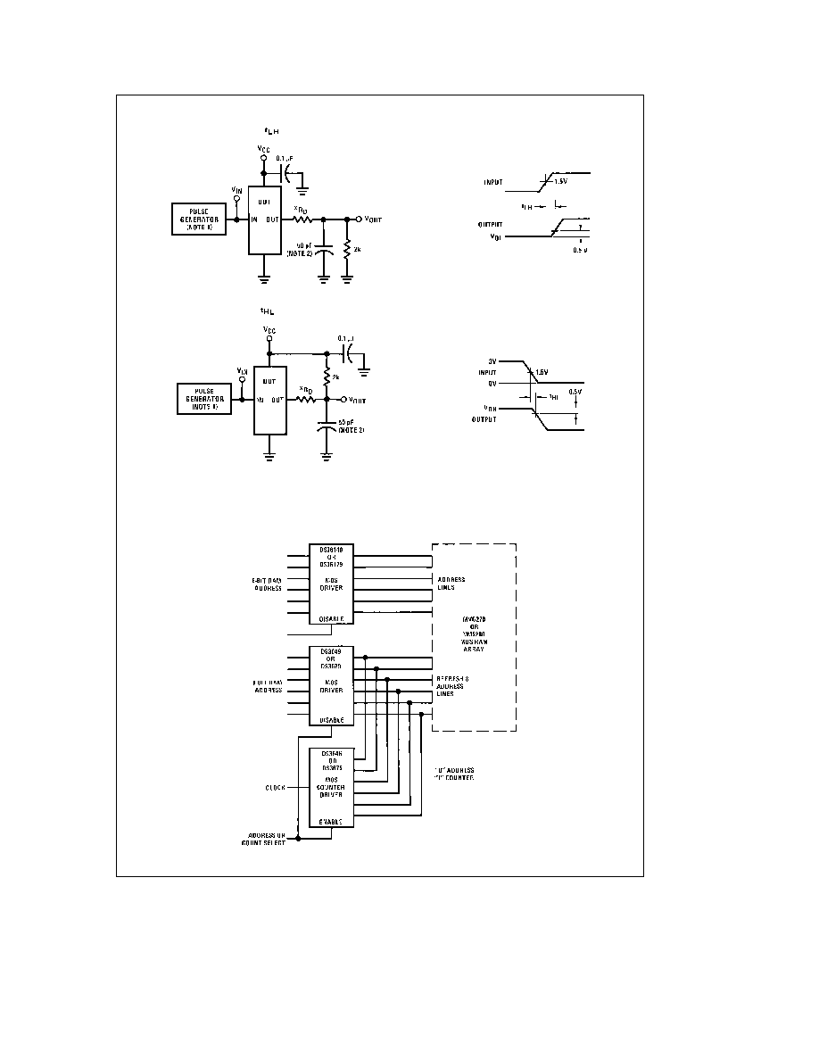
AC Test Circuits and Switching Time Waveforms
(Continued)
TL F 7553 ≠ 4
FIGURE 2
TL F 7553 ≠ 5
FIGURE 3
Internal on DS16149 and DS36149
Note 1
The pulse generator has the following characteristics Z
OUT
e
50 X and PRR
s
1 MHz Rise and fall times between 10% and 90% points
s
5 ns
Note 2
C
L
includes probe and jig capacitance
Typical Applications
TL F 7553 ≠ 6
4
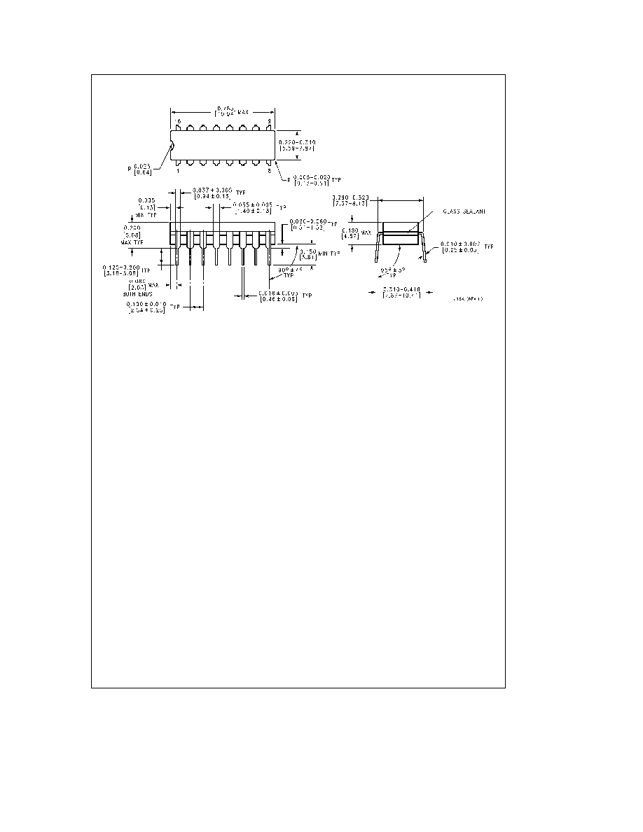
Physical Dimensions
inches (millimeters)
Ceramic Dual-In-Line Package (J)
Order Number DS16149J DS36149J
DS16179J or DS36179J
NS Package Number J16A
5