
TL F 5875
DS1628DS3628
Octal
TRI-STATE
MOS
Drivers
February 1986
DS1628 DS3628 Octal TRI-STATE
MOS Drivers
General Description
The DS1628 DS3628 are octal Schottky memory drivers
with TRI-STATE outputs designed to drive high capacitive
loads associated with MOS memory systems The drivers'
output (V
OH
) is specified at 3 4V to provide additional noise
immunity required by MOS inputs A PNP input structure is
employed to minimize input currents The circuit employs
Schottky-clamped transistors for high speed A NOR gate of
two inputs DIS1 and DIS2 controls the TRI-STATE mode
Features
Y
High speed capabilities
Typical 5 ns driving 50 pF
8 ns driving 500 pF
Y
TRI-STATE outputs
Y
High V
OH
(3 4V min)
Y
High density
Eight drivers and two disable controls for TRI-STATE
in a 20-pin package
Y
PNP inputs reduce DC loading on bus lines
Y
Glitch-free power up down
Schematic and Connection Diagrams
TL F 5875 � 1
(Equivalent Input Output Circuit)
Truth Table
Disable Input
Input
Output
DIS 1
DIS 2
H
H
X
Z
H
X
X
Z
X
H
X
Z
L
L
H
L
L
L
L
H
H
e
high level
L
e
low level
X
e
don't care
Z
e
high impedance (off)
Dual-In-Line Package
TL F 5875 � 2
Top View
Order Number
DS1628J DS3628J DS3628N
See NS Package Number J20A or N20A
Typical Application
TL F 5875 � 3
TRI-STATE
is a registered trademark of National Semiconductor Corp
C1995 National Semiconductor Corporation
RRD-B30M115 Printed in U S A
Absolute Maximum Ratings
(Note 1)
If Military Aerospace specified devices are required
please contact the National Semiconductor Sales
Office Distributors for availability and specifications
Supply Voltage
7 0V
Logical ``1'' Input Voltage
7 0V
Logical ``0'' Input Voltage
b
1 5V
Storage Temperature Range
b
65 C to
a
150 C
Maximum Power Dissipation at 25 C
Cavity Package
1667 mW
Molded Package
1832 mW
Lead Temperature (Soldering 10 seconds)
300 C
Derate cavity package 11 1 mW C above 25 C derate molded package
14 7 mW C above 25 C
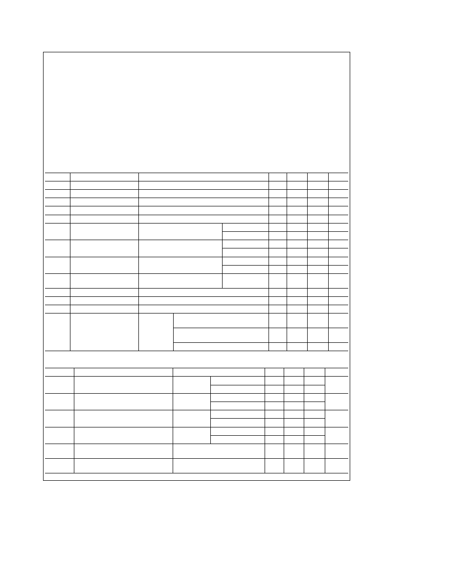
Operating Conditions
Min
Max
Units
Supply voltage (V
CC
)
4 5
5 5
V
Temperature (T
A
)
DS1628
b
55
a
125
C
DS3628
0
a
70
C
Electrical Characteristics
(Notes 2 3)
Symbol
Parameter
Conditions
Min
Typ
Max
Units
V
IN(1)
Logical ``1'' Input Voltage
2 0
V
V
IN(0)
Logical ``0'' Input Voltage
0 8
V
I
IN(1)
Logical ``1'' Input Current
V
CC
e
5 5V
V
IN
e
5 5V
0 1
40
m
A
I
IN(0)
Logical ``0'' Input Current
V
CC
e
5 5V
V
IN
e
5 5V
b
180
b
400
m
A
V
CLAMP
Input Clamp Voltage
V
CC
e
4 5V
I
IN
e b
18 mA
b
0 7
b
1 2
V
V
OH
Logical ``1'' Output Voltage
V
CC
e
4 5V I
OH
e b
10 mA
DS1628
3 4
4 3
V
(No Load)
DS3628
3 5
4 3
V
V
OL
Logical ``0'' Output Voltage
V
CC
e
4 5V I
OL
e
10 mA
DS1628
0 25
0 4
V
(No Load)
DS3628
0 25
0 35
V
V
OH
Logical ``1'' Output Voltage
V
CC
e
4 5V I
OH
e b
1 0 mA
DS1628
2 5
3 9
V
(With Load)
DS3628
2 7
3 9
V
V
OL
Logical ``0'' Output Voltage
V
CC
e
4 5V I
OL
e
20 mA
DS1628 DS3628
0 35
0 5
V
(With Load)
I
ID
Logical ``1'' Drive Current
V
CC
e
4 5V V
OUT
e
0V (Note 6)
b
150
mA
I
OD
Logical ``0'' Drive Current
V
CC
e
4 5V V
OUT
e
4 5V (Note 6)
150
mA
Hi-Z
TRI-STATE Output Current
V
OUT
e
0 4V to 2 4V DIS1 or DIS2
e
2 0V
b
40
0 1
40
m
A
I
CC
Power Supply Current
V
CC
e
5 5V
One DIS Input
e
3 0V
90
120
mA
All Other Inputs
e
X Outputs at Hi-Z
DIS1 DIS2
e
0V Others
e
3V
70
100
mA
Outputs on
All Inputs
e
0V Outputs Off
25
50
mA
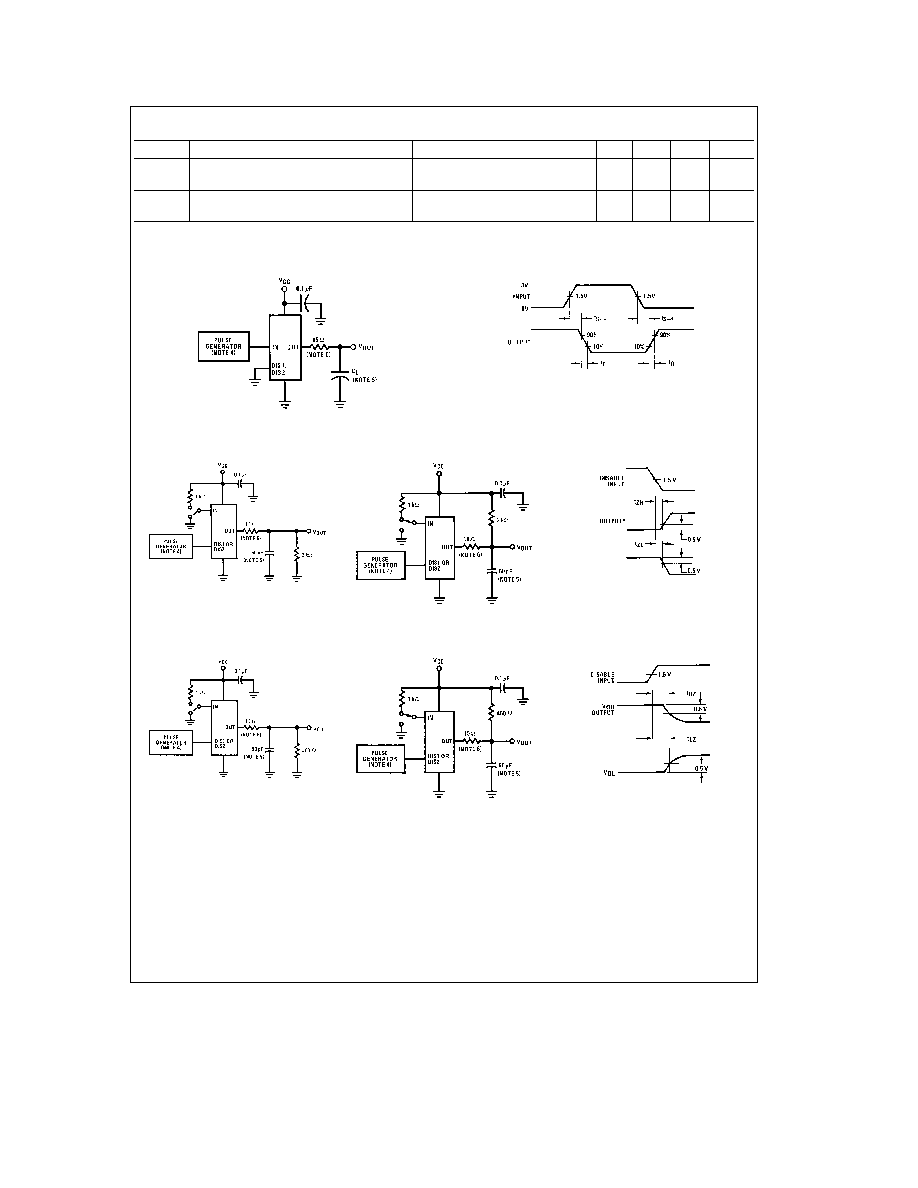
Switching Characteristics
(V
CC
e
5V T
A
e
25 C) (Note 6)
Symbol
Parameter
Conditions
Min
Typ
Max
Units
t
Sa b
Storage Delay Negative Edge
(
Figure 1 )
C
L
e
50 pF
4 0
5 0
ns
C
L
e
500 pF
6 5
8 0
t
Sb a
Storage Delay Positive Edge
(
Figure 1 )
C
L
e
50 pF
4 2
5 0
ns
C
L
e
500 pF
6 5
8 0
t
F
Fall Time
(
Figure 1 )
C
L
e
50 pF
4 2
6 0
ns
C
L
e
500 pF
19
22
t
R
Rise Time
(
Figure 1 )
C
L
e
50 pF
5 2
7 0
ns
C
L
e
500 pF
20
24
t
ZL
Delay from Disable Input to Logical ``0''
C
L
e
50 pF
R
L
e
2 kX to V
CC
19
25
ns
Level (from High Impedance State)
to GND
(
Figure 2 )
t
ZH
Delay from Disable Input to Logical ``1''
C
L
e
50 pF
R
L
e
2 kX to GND
13
20
ns
Level (from High Impedance State)
to GND
(
Figure 2 )
2
Switching Characteristics
(Continued) (V
CC
e
5V T
A
e
25 C) (Note 6)
Symbol
Parameter
Conditions
Min
Typ
Max
Units
t
LZ
Delay from Disable Input to High Impedance
C
L
e
50 pF
R
L
e
400X to V
CC
18
25
ns
State (from Logical ``0'' Level)
to GND
(
Figure 3 )
t
HZ
Delay from Disable Input to High Impedance
C
L
e
50 pF
R
L
e
400X to GND
8 5
15
ns
State (from Logical ``1'' Level)
to GND
(
Figure 3 )
AC Test Circuits and Switching Time Waveforms
t
Sa b
t
Sb a
t
r
t
f
TL F 5875 � 4
TL F 5875 � 5
FIGURE 1
t
ZH
TL F 5875 � 6
t
ZL
TL F 5875 � 7
TL F 5875 � 8
ANY ONE OF EIGHT OUTPUTS
FIGURE 2
t
HZ
TL F 5875 � 9
t
LZ
TL F 5875 � 10
TL F 5875 � 11
FIGURE 3
Note 1
``Absolute Maximum Ratings'' are those values beyond which the safety of the device cannot be guaranteed Except for ``Operating Temperature Range''
they are not meant to imply that the devices should be operated at these limits The table of ``Electrical Characteristics'' provides conditions for actual device
operation
Note 2
Unless otherwise specified min max limits apply across the
b
55 C to
a
125 C temperature range for the DS1628 and across the 0 C to
a
70 C range for
the DS3628 All typical values are for T
A
e
25 C and V
CC
e
5V
Note 3
All currents into device pins shown as positive all currents out of device pins shown as negative all voltages references to ground unless otherwise noted
All values shown as max or min on absolute value basis
Note 4
The pulse generator has the following characteristics Z
OUT
e
50X and PRR
s
1 mHz Rise and fall times between 10% and 90% points
s
5 ns
Note 5
C
L
includes probe and jig capacitance
Note 6
When measuring output drive current and switching response for the DS1628 and DS3628 a 15X resistor should be placed in series with each output
3

DS1628DS3628
Octal
TRI-STATE
MOS
Drivers
Physical Dimensions
inches (millimeters)
Ceramic Dual-In-Line Package (J)
Order Number DS1628J or DS3628J
NS Package Number J20A
Molded Dual-In-Line Package (N)
Order Number DS3628N
NS Package Number N20A
LIFE SUPPORT POLICY
NATIONAL'S PRODUCTS ARE NOT AUTHORIZED FOR USE AS CRITICAL COMPONENTS IN LIFE SUPPORT
DEVICES OR SYSTEMS WITHOUT THE EXPRESS WRITTEN APPROVAL OF THE PRESIDENT OF NATIONAL
SEMICONDUCTOR CORPORATION As used herein
1 Life support devices or systems are devices or
2 A critical component is any component of a life
systems which (a) are intended for surgical implant
support device or system whose failure to perform can
into the body or (b) support or sustain life and whose
be reasonably expected to cause the failure of the life
failure to perform when properly used in accordance
support device or system or to affect its safety or
with instructions for use provided in the labeling can
effectiveness
be reasonably expected to result in a significant injury
to the user
National Semiconductor
National Semiconductor
National Semiconductor
National Semiconductor
Corporation
Europe
Hong Kong Ltd
Japan Ltd
1111 West Bardin Road
Fax (a49) 0-180-530 85 86
13th Floor Straight Block
Tel 81-043-299-2309
Arlington TX 76017
Email cnjwge tevm2 nsc com
Ocean Centre 5 Canton Rd
Fax 81-043-299-2408
Tel 1(800) 272-9959
Deutsch Tel (a49) 0-180-530 85 85
Tsimshatsui Kowloon
Fax 1(800) 737-7018
English
Tel (a49) 0-180-532 78 32
Hong Kong
Fran ais Tel (a49) 0-180-532 93 58
Tel (852) 2737-1600
Italiano
Tel (a49) 0-180-534 16 80
Fax (852) 2736-9960
National does not assume any responsibility for use of any circuitry described no circuit patent licenses are implied and National reserves the right at any time without notice to change said circuitry and specifications