DS3662
Quad High Speed Trapezoidal
TM
Bus Transceiver
General Description
The DS3662 is a quad high speed Schottky bus transceiver
intended for use with terminated 120
impedance lines. It is
specifically designed to reduce noise in unbalanced trans-
mission systems. The open collector drivers generate pre-
cise trapezoidal waveforms with rise and fall times of 15 ns
(typical), which are relatively independent of capacitive load-
ing conditions on the outputs. This reduces noise coupling to
the adjacent lines without any appreciable impact on the
maximum data rate obtainable with high speed bus trans-
ceivers. In addition, the receivers use a low pass filter in con-
junction with a high speed comparator, to further enhance
the noise immunity. Tightly controlled threshold levels on the
receiver provide equal rejection to both negative and positive
going noise pulses on the bus.
The external termination is intended to be a 180
resistor
from the bus to 5V logic supply, together with a 390
resistor
from the bus to ground. The bus can be terminated at one or
both ends. A two input NOR gate is provided to disable all
drivers in a package simultaneously.
Features
n
Pin to pin functional replacement for DS8641
n
Guaranteed AC specifications on noise immunity and
propagation delay over the specified temperature and
supply voltage range
n
Temperature insensitive receiver thresholds track bus
logic level
n
Trapezoidal bus waveforms reduce noise coupling to
adjacent lines
n
Precision receiver thresholds provide maximum noise
immunity and symmetrical response to positive and
negative going pulses
n
Open collector driver output allows wire-OR connection
n
High speed Schottky technology
n
15 �A typical bus termination current with normal V
CC
or
with V
CC
= 0V
n
Glitch free power up/down protection on the driver
output
n
TTL compatible driver and disable inputs, and receiver
outputs
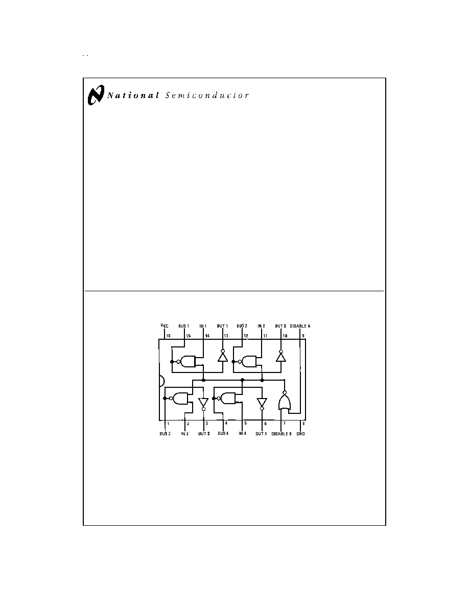
Block and Connection Diagram
Trapezoidal
TM
is a trademark of National Semiconductor Corp.
Dual-In-Line Package
DS005803-1
Top View
Order Number DS3662J, DS3662N or DS3662WM
See NS Package Number J16A, N16A or M16B
July 1992
DS3662
Quad
High
Speed
T
rapezoidal
Bus
T
ransceiver
� 1999 National Semiconductor Corporation
DS005803
www.national.com
Absolute Maximum Ratings
(Note 2)
If Military/Aerospace specified devices are required,
please contact the National Semiconductor Sales Office/
Distributors for availability and specifications.
Supply Voltage
7V
Input and Output Voltage
5.5V
Storage Temperature Range
-65�C to +150�C
Maximum Power Dissipation (Note 1) at 25�C
Cavity Package
1509 mW
Molded Package
1476 mW
Lead Temperature (Soldering, 4 sec.)
260�C
Recommended Operating
Conditions
Min
Max
Units
Supply Voltage (V
CC
)
4.75
5.25
V
Temperature Range (T
A
)
0
70
�C
Note 1:
Derate cavity package 10.1 mW/�C above 25�C; derate molded
package 11.8 mW/�C above 25�C.
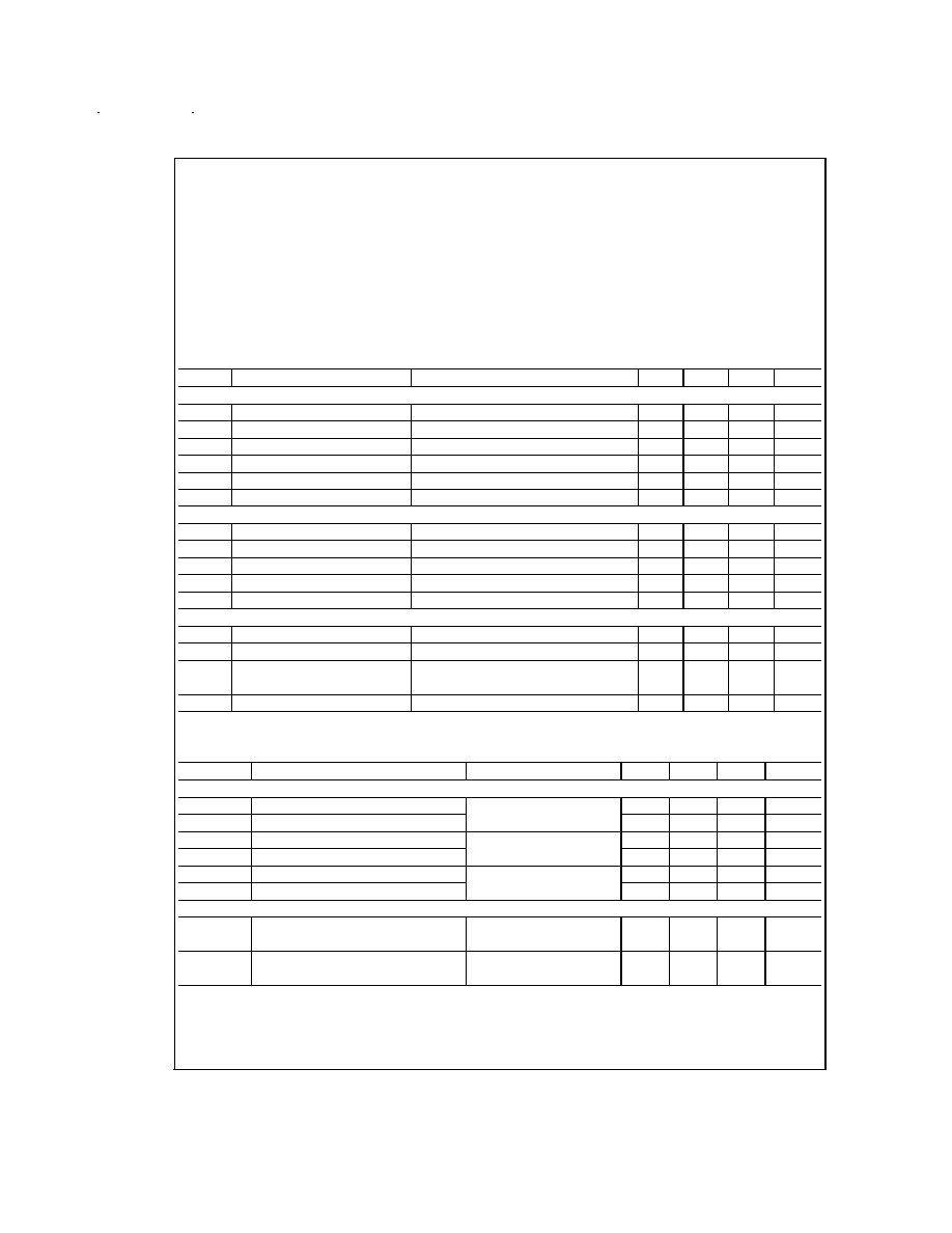
Electrical Characteristics
(Notes 3, 4)
Symbol
Parameter
Conditions
Min
Typ
Max
Units
DRIVER AND DISABLE INPUTS
V
IH
Logical "1" Input Voltage
2.0
V
V
IL
Logical "0" Input Voltage
0.8
V
I
I
Logical "1" Input Current
V
IN
= 5.5V
1
mA
I
IH
Logical "1" Input Current
V
IN
= 2.4V
40
�A
I
IL
Logical "0" Input Current
V
IN
= 0.4V
-1
-1.6
mA
V
CL
Input Diode Clamp Voltage
I
CLAMP
= -12 mA
-0.8
-1.5
V
DRIVER OUTPUT/RECEIVER INPUT
V
OLB
Low Level Bus Voltage
V
DIS
= 0.8V, V
IN
= 2V, I
BUS
= 100 mA
0.6
0.9
V
I
IHB
Maximum Bus Current
V
IN
= 0.8V, V
BUS
= 4V, V
CC
= 5.25V
10
100
�A
I
ILB
Maximum Bus Current
V
IN
= 0.8V, V
BUS
= 4V, V
CC
= 0V
100
�A
V
IH
High Level Receiver Threshold
V
IN
= 0.8V, V
OL
= 16 mA
1.90
1.70
V
V
IL
Low Level Receiver Threshold
V
IN
= 0.8V, I
OH
= -400 �A
1.70
1.50
V
RECEIVER OUTPUT
V
OH
Logical "1" Output Voltage
V
IN
= 0.8V, V
BUS
= 0.5V, I
OH
= -400 �A
2.4
3.2
V
V
OL
Logical "0" Output Voltage
V
IN
= 0.8V, V
BUS
= 4V, I
OL
= 16 mA
0.35
0.5
V
I
OS
Output Short Circuit Current
V
DIS
= 0.8V, V
IN
= 0.8V, V
BUS
= 0.5V,
-40
-70
-100
mA
V
OS
= 0V, V
CC
= 5.25V, (Note 5)
I
CC
Supply Current
V
DIS
= 0V, V
IN
= 2V
50
90
mA
Switching Characteristics
(Notes 3, 4)
Symbol
Parameter
Conditions
Min
Typ
Max
Units
PROPAGATION DELAYS
t
PLHD
Disable to Bus "1"
Figure 1
25
35
ns
t
PHLD
Disable to Bus "0"
25
35
ns
t
PLHB
Driver Input to Bus "1"
Figure 2
20
30
ns
t
PHLB
Driver Input to Bus "0"
20
30
ns
t
PLHR
Bus to Logical "1" Receiver Output
Figure 3
25
40
ns
t
PHLR
Bus to Logical "0" Receiver Output
25
40
ns
NOISE IMMUNITY
t
rB
, t
fB
Rise and Fall Times (10%�90%)
Figure 2
10
15
20
ns
of the Driver Output
t
nR
Receiver Noise Rejection
No Response at Receiver
20
10
ns
Pulse Width
Output as per
Figure 4
Note 2: "Absolute Maximum Ratings" are those values beyond which the safety of the device cannot be guaranteed. They are not meant to imply that the devices
should be operated at these limits. The tables of "Electrical Characteristics" and "Recommended Operating Conditions" provide conditions for actual device operation.
Note 3: Unless otherwise specified min/max limits apply across the supply and temperature range listed in the table of "Recommended Operating Conditions". All
typical values are for T
A
= 25�C and V
CC
= 5V.
Note 4: All currents into device pins shown as positive, out of device pins as negative, all voltages referenced to ground unless otherwise noted. All values shown
as max or min on absolute value basis.
www.national.com
2
Switching Characteristics
(Notes 3, 4) (Continued)
Note 5: Only one output at a time should be shorted.
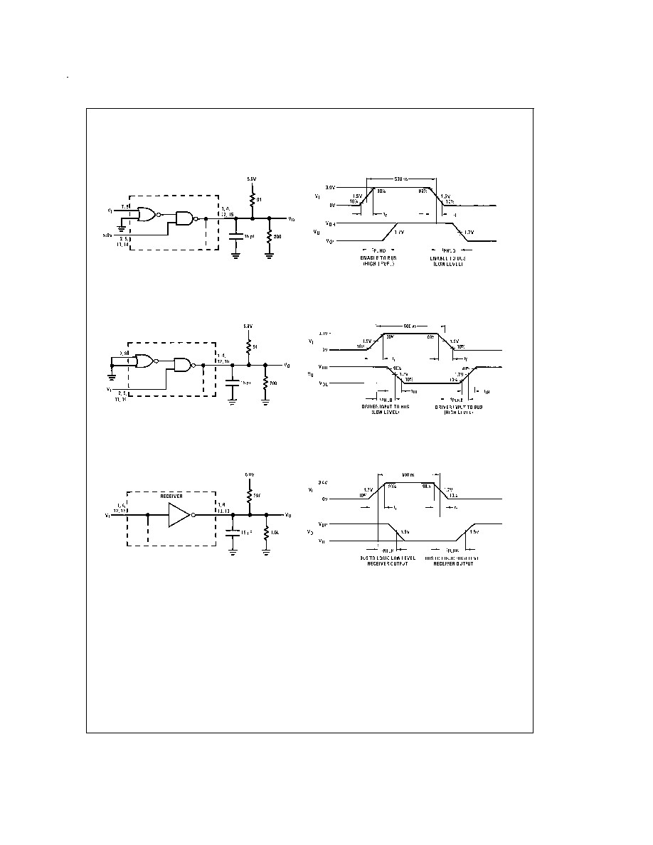
AC Test Circuits and Switching Waveforms
DS005803-2
DS005803-3
Note: t
r
= t
f
= 2.5 ns. Pulse width = 500 ns measured between 1.5V levels. f = 1 MHz.
FIGURE 1. Disable Delays
DS005803-4
DS005803-5
Note: t
r
= t
f
= 2.5 ns. Pulse width = 500 ns measured between 1.5V levels. f = 1 MHz.
FIGURE 2. Driver Propagation Delays
DS005803-6
DS005803-7
Note: t
r
= t
f
= 15 ns. Pulse width = 500 ns measured between 1.7V levels. f = 1 MHz.
FIGURE 3. Receiver Propagation Delays
www.national.com
3
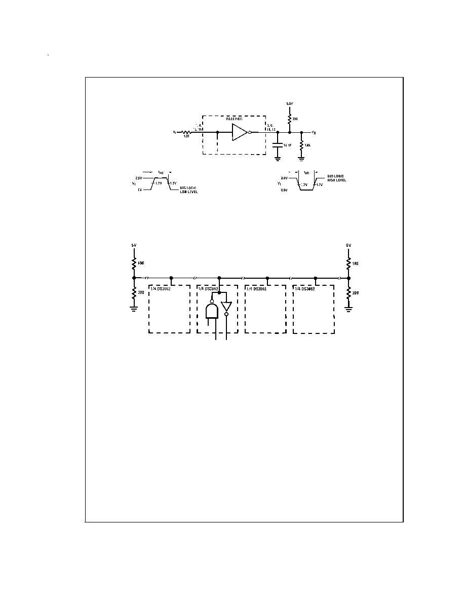
AC Test Circuits and Switching Waveforms
(Continued)
Typical Application
DS005803-8
DS005803-9
t
r
= t
f
= 2.5 ns
(a) Receiver Output (V
O
) to Remain Greater than 2.2V
DS005803-10
t
r
= t
f
= 2.5 ns
(b) Receiver Output (V
O
) to Remain Less than 0.7V
FIGURE 4. Receiver Noise Immunity: "No Response at Output" Input Waveforms
DS005803-11
www.national.com
4
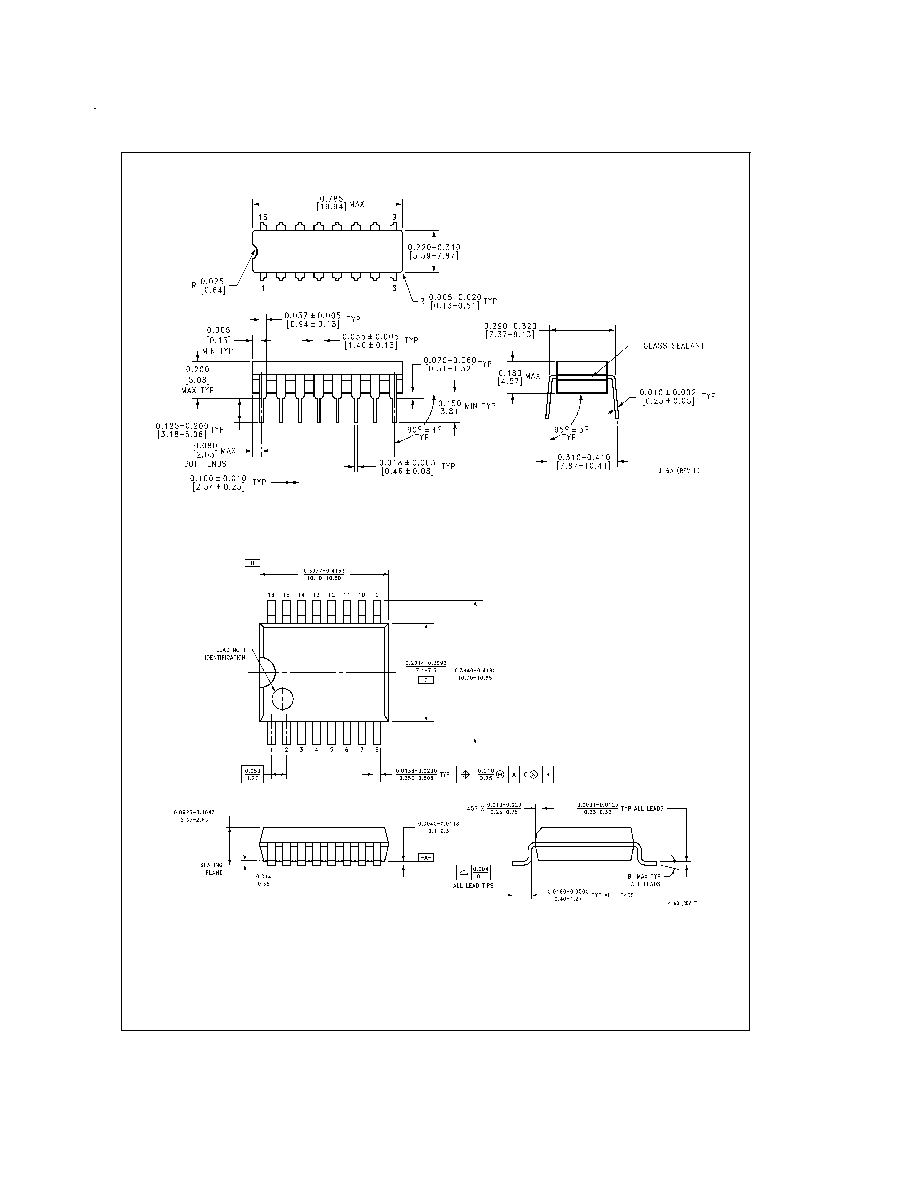
Physical Dimensions
inches (millimeters) unless otherwise noted
Ceramic Dual-In-Line Package (J)
Order Number DS3662J
NS Package Number J16A
16-Lead Molded Small Outline Package (M)
Order Number DS3662WM
NS Package Number M16B
www.national.com
5