DS90CR481 / DS90CR482 48-Bit LVDS Channel Link SER/DES - 65 - 112 MHz
DS90CR481 / DS90CR482
48-Bit LVDS Channel Link SER/DES - 65 - 112 MHz
General Description
The DS90CR481 transmitter converts 48 bits of CMOS/TTL
data into eight LVDS (Low Voltage Differential Signaling)
data streams. A phase-locked transmit clock is transmitted in
parallel with the data streams over a ninth LVDS link. Every
cycle of the transmit clock 48 bits of input data are sampled
and transmitted. The DS90CR482 receiver converts the
LVDS data streams back into 48 bits of LVCMOS/TTL data.
At a transmit clock frequency of 112MHz, 48 bits of TTL data
are transmitted at a rate of 672Mbps per LVDS data channel.
Using a 112MHz clock, the data throughput is 5.38Gbit/s
(672Mbytes/s). At a transmit clock frequency of 112MHz, 48
bits of TTL data are transmitted at a rate of 672Mbps per
LVDS data channel. Using a 66MHz clock, the data through-
put is 3.168Gbit/s (396Mbytes/s).
The multiplexing of data lines provides a substantial cable
reduction. Long distance parallel single-ended buses typi-
cally require a ground wire per active signal (and have very
limited noise rejection capability). Thus, for a 48-bit wide
data and one clock, up to 98 conductors are required. With
this Channel Link chipset as few as 19 conductors (8 data
pairs, 1 clock pair and a minimum of one ground) are
needed. This provides an 80% reduction in cable width,
which provides a system cost savings, reduces connector
physical size and cost, and reduces shielding requirements
due to the cables' smaller form factor.
The 48 CMOS/TTL inputs can support a variety of signal
combinations. For example, 6 8-bit words or 5 9-bit (byte +
parity) and 3 controls.
The DS90CR481/DS90CR482 chipset is improved over prior
generations of Channel Link devices and offers higher band-
width support and longer cable drive with three areas of
enhancement. To increase bandwidth, the maximum clock
rate is increased to 112 MHz and 8 serialized LVDS outputs
are provided. Cable drive is enhanced with a user selectable
pre-emphasis feature that provides additional output current
during transitions to counteract cable loading effects. Op-
tional DC balancing on a cycle-to-cycle basis, is also pro-
vided to reduce ISI (Inter-Symbol Interference). With pre-
emphasis and DC balancing, a low distortion eye-pattern is
provided at the receiver end of the cable. A cable deskew
capability has been added to deskew long cables of pair-to-
pair skew of up to +/-1 LVDS data bit time (up to 80 MHz
Clock Rate). These three enhancements allow cables 5+
meters in length to be driven.
The chipset is an ideal means to solve EMI and cable size
problems associated with wide, high speed TTL interfaces.
Features
n
3.168 Gbits/sec bandwidth with 66 MHz Clock
n
5.376 Gbits/sec bandwidth with 112 MHz Clock
n
65 - 112 MHz input clock support
n
LVDS SER/DES reduces cable and connector size
n
Pre-emphasis reduces cable loading effects
n
Optional DC balance encoding reduces ISI distortion
n
Cable Deskew of +/-1 LVDS data bit time (up to 80
MHz Clock Rate)
n
5V Tolerant TxIN and control input pins
n
Flow through pinout for easy PCB design
n
+3.3V supply voltage
n
Transmitter rejects cycle-to-cycle jitter
n
Conforms to ANSI/TIA/EIA-644-1995 LVDS Standard
Generalized Block Diagrams (DS90CR481 and DS90CR482)
20009101
May 2002
DS90CR481/DS90CR482
48-Bit
L
VDS
Channel
Link
SER/DES
6
5
-
1
12
MHz
© 2002 National Semiconductor Corporation
DS200091
www.national.com
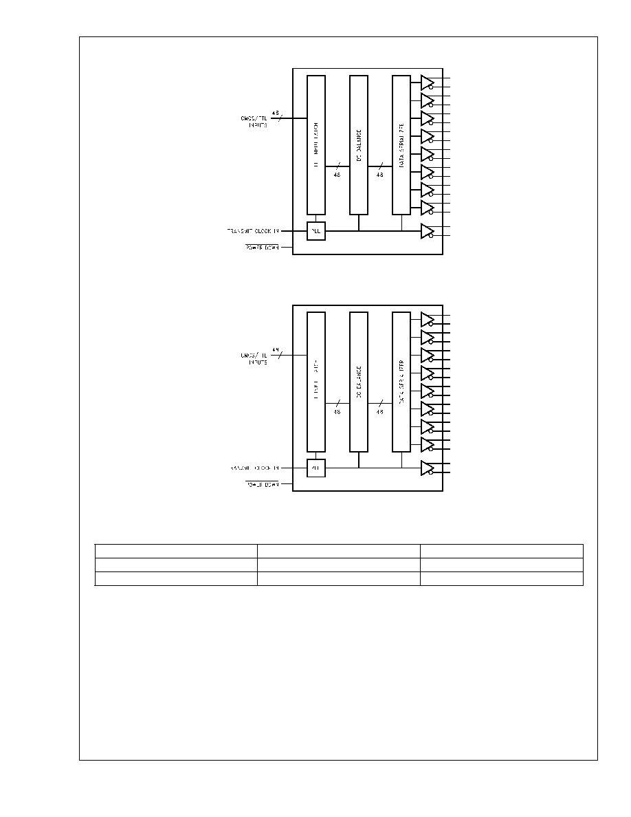
Generalized Transmitter Block Diagram DS90CR481
20009102
Generalized Receiver Block Diagram DS90CR482
20009102
Ordering Information
Order Number
Function
Package
DS90CR481VJD
Transmitter (Serializer)
VJD100A
DS90CR482VS
Receiver (Deserializer)
VJD100A
DS90CR481/DS90CR482
www.national.com
2
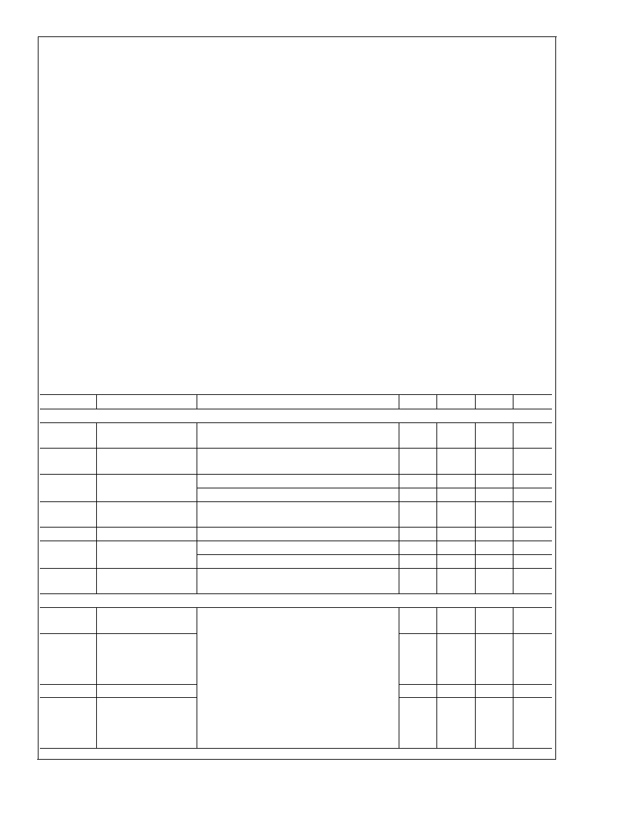
Absolute Maximum Ratings
(Note 1)
If Military/Aerospace specified devices are required,
please contact the National Semiconductor Sales Office/
Distributors for availability and specifications.
Supply Voltage (V
CC
)
-0.3V to +4V
CMOS/TTL Input Voltage
-0.3V to +5.5V
LVCMOS/TTL Output
Voltage
-0.3V to (V
CC
+ 0.3V)
LVDS Receiver Input
Voltage
-0.3V to +3.6V
LVDS Driver Output
Voltage
-0.3V to +3.6V
LVDS Output Short
Circuit Duration
Continuous
Junction Temperature
+150°C
Storage Temperature
-65°C to +150°C
Lead Temperature
(Soldering, 4 sec.)
100L TQFP
+260°C
Maximum Package Power Dissipation Capacity
@
25°C
100 TQFP Package:
DS90CR481VJD
2.3W
DS90CR482VS
2.3W
Package Derating:
DS90CR481VJD
18.1mW/°C above +25°C
DS90CR482VS
18.1mW/°C above +25°C
ESD Rating:
DS90CR481
(HBM, 1.5k
, 100pF)
>
6 kV
(EIAJ, 0
, 200pF)
>
300 V
DS90CR482
(HBM, 1.5k
, 100pF)
>
2 kV
(EIAJ, 0
, 200pF)
>
200 V
Recommended Operating
Conditions
Min
Nom
Max
Units
Supply Voltage (V
CC
)
3.0
3.3
3.6
V
Operating Free Air
Temperature (T
A)
-10
+25
+70
°C
Supply Noise Voltage
100
mV
p-p
Input Clock (TX)
65
112
MHz
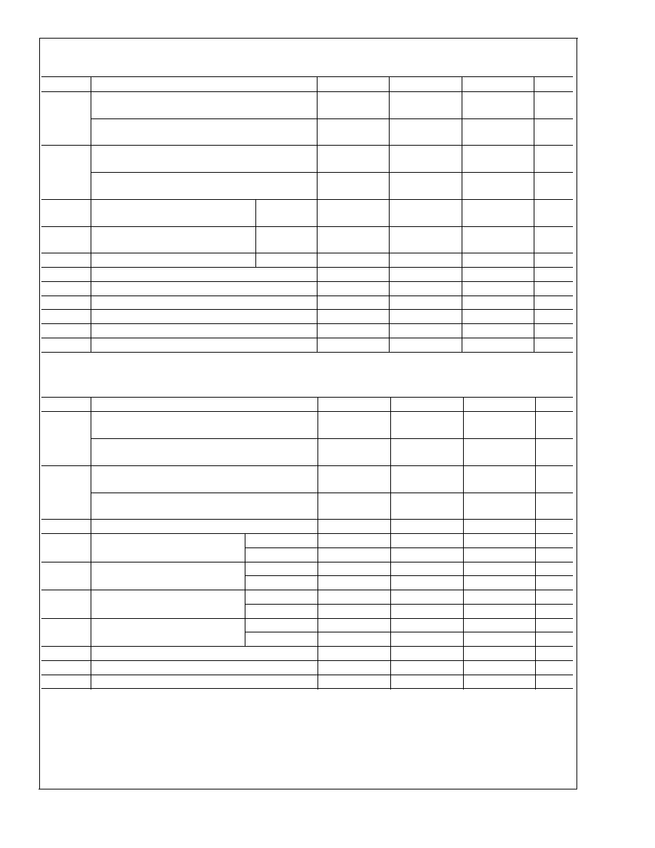
Electrical Characteristics
Over recommended operating supply and temperature ranges unless otherwise specified.
Symbol
Parameter
Conditions
Min
Typ
Max
Units
CMOS/TTL DC SPECIFICATIONS
V
IH
High Level Input
Voltage
2.0
V
V
IL
Low Level Input
Voltage
GND
0.8
V
V
OH
High Level Output
Voltage
I
OH
= -0.4 mA
2.7
2.9
V
I
OH
= -2mA
2.7
2.85
V
V
OL
Low Level Output
Voltage
I
OL
= 2 mA
0.1
0.3
V
V
CL
Input Clamp Voltage
I
CL
= -18 mA
-0.79
-1.5
V
I
IN
Input Current
V
IN
= 0.4V, 2.5V or V
CC
+1.8
+15
µA
V
IN
= GND
-15
0
µA
I
OS
Output Short Circuit
Current
V
OUT
= 0V
-120
mA
LVDS DRIVER DC SPECIFICATIONS
|V
OD
|
Differential Output
Voltage
R
L
= 100
250
345
450
mV
V
OD
Change in V
OD
between
Complimentary Output
States
35
mV
V
OS
Offset Voltage
1.125
1.25
1.375
V
V
OS
Change in V
OS
between
Complimentary Output
States
35
mV
DS90CR481/DS90CR482
www.national.com
3
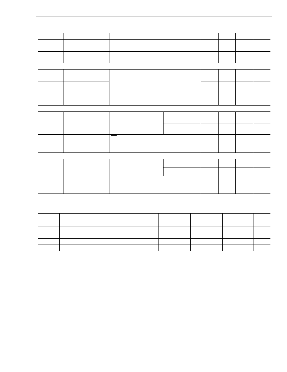
Electrical Characteristics
(Continued)
Over recommended operating supply and temperature ranges unless otherwise specified.
Symbol
Parameter
Conditions
Min
Typ
Max
Units
I
OS
Output Short Circuit
Current
V
OUT
= 0V, R
L
= 100
-3.5
-5
mA
I
OZ
Output TRI-STATE
Current
PD = 0V, V
OUT
= 0V or V
CC
±
1
±
10
µA
LVDS RECEIVER DC SPECIFICATIONS
V
TH
Differential Input High
Threshold
V
CM
= +1.2V
+100
mV
V
TL
Differential Input Low
Threshold
-100
mV
I
IN
Input Current
V
IN
= +2.4V, V
CC
= 3.6V
±
10
µA
V
IN
= 0V, V
CC
= 3.6V
±
10
µA
TRANSMITTER SUPPLY CURRENT
ICCTW
Transmitter Supply
Current
Worst Case
R
L
= 100
, C
L
= 5 pF,
BAL = High,
Worst Case Pattern
(
Figures 1, 2)
f = 66MHz
106
160
mA
f = 112MHz
155
210
mA
ICCTZ
Transmitter Supply
Current
Power Down
PD = Low
5
50
µA
Driver Outputs in TRI-STATE during power down
Mode
RECEIVER SUPPLY CURRENT
ICCRW
Receiver Supply
Current
Worst Case
C
L
= 8 pF, BAL = High,
Worst Case Pattern
(
Figures 1, 3)
f = 66MHz
200
210
mA
f = 112MHz
250
280
mA
ICCRZ
Receiver Supply
Current
Power Down
PD = Low
Receiver Outputs stay low during power down
mode.
20
100
µA
Recommended Transmitter Input Characteristics
Over recommended operating supply and temperature ranges unless otherwise specified.
Symbol
Parameter
Min
Typ
Max
Units
TCIT
TxCLK IN Transition Time (
Figure 4)
1.0
2.0
3.0
ns
TCIP
TxCLK IN Period (
Figure 5)
8.93
15.38
ns
TCIH
TxCLK in High Time (
Figure 5)
0.35T
0.5T
0.65T
ns
TCIL
TxCLK in Low Time (
Figure 5)
0.35T
0.5T
0.65T
ns
TXIT
TxIN Transition Time
1.5
6.0
ns
DS90CR481/DS90CR482
www.national.com
4
Transmitter Switching Characteristics
Over recommended operating supply and temperature ranges unless otherwise specified.
Symbol
Parameter
Min
Typ
Max
Units
LLHT
LVDS Low-to-High Transition Time, (
Figure 2),
PRE = 0.75V (disabled)
0.14
0.7
ns
LVDS Low-to-High Transition Time, (
Figure 2),
PRE = Vcc (max)
0.11
0.6
ns
LHLT
LVDS High-to-Low Transition Time, (
Figure 2),
PRE = 0.75V (disabled)
0.16
0.8
ns
LVDS High-to-Low Transition Time, (
Figure 2),
PRE = Vcc (max)
0.11
0.7
ns
TBIT
Transmitter Bit Width
f = 66 MHz,
112MHz
1/7 TCIP
ns
TPPOS
Transmitter Pulse Positions -
Normalized
f = 65 to 112
MHz
- 200
0
+200
ps
TJCC
Tranmitter Jitter - Cycle-to-Cycle
100
ps
TCCS
TxOUT Channel to Channel Skew
40
ps
TSTC
TxIN Setup to TxCLK IN, (
Figure 5)
2.5
ns
THTC
TxIN Hold to TxCLK IN, (
Figure 5)
0
ns
TPDL
Transmitter Propagation Delay - Latency, (
Figure 7)
1.5(TCIP)+3.72
1.5(TCIP)+4.4
1.5(TCIP)+6.24
ns
TPLLS
Transmitter Phase Lock Loop Set, (
Figure 9)
10
ms
TPDD
Transmitter Powerdown Delay, (
Figure 11)
100
ns
Receiver Switching Characteristics
Over recommended operating supply and temperature ranges unless otherwise specified.
Symbol
Parameter
Min
Typ
Max
Units
CLHT
CMOS/TTL Low-to-High Transition Time, Rx data out,
(
Figure 3)
2.0
ns
CMOS/TTL Low-to-High Transition Time, Rx clock
out, (
Figure 3)
1.0
ns
CHLT
CMOS/TTL High-to-Low Transition Time, Rx data out,
(
Figure 3)
2.0
ns
CMOS/TTL High-to-Low Transition Time, Rx clock
out, (
Figure 3)
1.0
ns
RCOP
RxCLK OUT Period, (
Figure 6)
8.928
T
15.38
ns
RCOH
RxCLK OUT High Time, (
Figure 6),
(Note 4)
f = 112 MHz
3.5
ns
f = 66 MHz
6.0
ns
RCOL
RxCLK OUT Low Time, (
Figure 6),
(Note 4)
f = 112 MHz
3.5
ns
f = 66 MHz
6.0
ns
RSRC
RxOUT Setup to RxCLK
OUT,(
Figure 6)
f = 112 MHz
2.4
ns
f = 66 MHz
3.6
ns
RHRC
RxOUT Hold to RxCLK OUT,
(
Figure 6), (Note 4)
f = 112 MHz
3.4
ns
f = 66 MHz
6.0
ns
RPDL
Receiver Propagation Delay - Latency, (
Figure 8)
3(TCIP)+4.0
3(TCIP)+4.8
3(TCIP)+6.5
ns
RPLLS
Receiver Phase Lock Loop Set, (
Figure 10)
10
ms
RPDD
Receiver Powerdown Delay, (
Figure 12)
1
µs
DS90CR481/DS90CR482
www.national.com
5
Document Outline