 | –≠–ª–µ–∫—Ç—Ä–æ–Ω–Ω—ã–π –∫–æ–º–ø–æ–Ω–µ–Ω—Ç: HC646 | –°–∫–∞—á–∞—Ç—å:  PDF PDF  ZIP ZIP |
TL F 5345
MM54HC646MM74HC646
Non-Inverting
Octal
Bus
TransceiverRegisters
MM54HC648MM74HC648
Inverting
Octal
Bus
TransceiverRegisters
January 1988
MM54HC646 MM74HC646 Non-Inverting
Octal Bus Transceiver Registers
MM54HC648 MM74HC648
Inverting Octal Bus Transceiver Registers
General Description
These transceivers utilize advanced silicon-gate CMOS
technology and contain two sets of TRI-STATE
outputs
two sets of D-type flip-flops and control circuitry designed
for high speed multiplexed transmission of data
Six control inputs enable this device to be used as a latched
transceiver unlatched transceiver or a combination of both
As a latched transceiver data from one bus is stored for
later retrieval by the other bus Alternately real time bus
data (unlatched) may be directly transferred from one bus to
another
Circuit operation is determined by the G DIR CAB CBA
SAB SBA control inputs The enable input G controls
whether any bus outputs are enabled The direction control
DIR determines which bus is enabled and hence the direc-
tion data flows The SAB SBA inputs control whether the
latched data (stored in D type flip flops) or the bus data
(from other bus input pins) is transferred Each set of flip-
flops has its own clock CAB and CBA for storing data Data
is latched on the rising edge of the clock
Each output can drive up to 15 low power Schottky TTL
loads These devices are functionally and pin compatible to
their LS-TTL counterparts All inputs are protected from
damage due to static discharge by diodes to V
CC
and
ground
Features
Y
Typical propagation delay 14 ns
Y
TRI-STATE outputs
Y
Bidirectional communication
Y
Wide power supply range 2 ≠ 6V
Y
Low quiescent supply current 160 mA
maximum (74HC)
Y
High output current 6 mA (74HC)
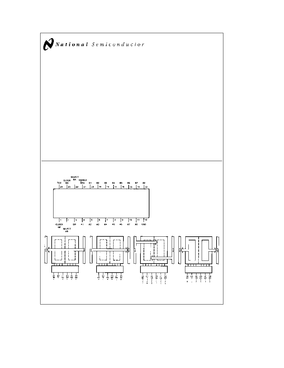
Connection Diagram
Dual-In-Line Package
TL F 5345 ≠ 2
Order Number MM54HC646 648 or
MM74HC646 648
TL F 5345 ≠ 1
Real-Time Transfer
Bus B to Bus A
Real-Time Transfer
Bus A to Bus B
Storage from
A B or A and B
Transfer Stored Data
to A or B
TRI-STATE
is a registered trademark of National Semiconductor Corp
C1995 National Semiconductor Corporation
RRD-B30M105 Printed in U S A
Absolute Maximum Ratings
(Notes 1
2)
If Military Aerospace specified devices are required
please contact the National Semiconductor Sales
Office Distributors for availability and specifications
Supply Voltage (V
CC
)
b
0 5 to
a
7 0V
DC Input Voltage (V
IN
)
b
1 5 to V
CC
a
1 5V
DC Output Voltage (V
OUT
)
b
0 5 to V
CC
a
0 5V
Clamp Diode Current (I
IK
I
OK
)
g
20 mA
DC Output Current per pin (I
OUT
)
g
35 mA
DC V
CC
or GND Current per pin (I
CC
)
g
70 mA
Storage Temperature Range (T
STG
)
b
65 C to
a
150 C
Power Dissipation (P
D
)
(Note 3)
600 mW
S O Package only
500 mW
Lead Temp (T
L
) (Soldering 10 seconds)
260 C
Operating Conditions
Min
Max
Units
Supply Voltage (V
CC
)
2
6
V
DC Input or Output Voltage
0
V
CC
V
(V
IN
V
OUT
)
Operating Temp Range (T
A
)
MM74HC
b
40
a
85
C
MM54HC
b
55
a
125
C
Input Rise or Fall Times
V
CC
e
2 0V
(t
r
t
f
)
1000
ns
V
CC
e
4 5V
500
ns
V
CC
e
6 0V
400
ns
DC Electrical Characteristics
(Note 4)
T
A
e
25 C
74HC
54HC
Symbol
Parameter
Conditions
V
CC
T
A
e b
40 to 85 C
T
A
e b
55 to 125 C
Units
Typ
Guaranteed Limits
V
IH
Minimum High Level
V
V
Input Voltage
V
V
V
V
V
IL
Maximum Low Level
V
V
Input Voltage
V
V
V
V
V
OH
Minimum High Level
V
IN
e
V
IH
or V
IL
Output Voltage
l
I
OUT
l
s
m
A
V
V
V
V
V
V
V
IN
e
V
IH
or V
IL
l
I
OUT
l
s
mA
V
V
l
I
OUT
l
s
mA
V
V
V
OL
Maximum Low Level
V
IN
e
V
IH
or V
IL
Output Voltage
l
I
OUT
l
s
m
A
V
V
V
V
V
V
V
IN
e
V
IH
or V
IL
l
I
OUT
l
s
mA
V
V
l
I
OUT
l
s
mA
V
V
I
IN
Maximum Input Current
V
IN
e
V
CC
or GND
V
g
g
g
m
A
I
OZ
Maximum TRI STATE
V
OUT
e
V
CC
or GND
V
g
g
g
m
A
Output Leakage
G
e
V
IH
I
CC
Maximum Quiescent
V
IN
e
V
CC
or GND
V
m
A
Supply Current
I
OUT
e
m
A
Note 1
Absolute Maximum Ratings are those values beyond which damage to the device may occur
Note 2
Unless otherwise specified all voltages are referenced to ground
Note 3
Power Dissipation temperature derating
plastic ``N'' package
b
12 mW C from 65 C to 85 C ceramic ``J'' package
b
12 mW C from 100 C to 125 C
Note 4
For a power supply of 5V
g
10% the worst case output voltages (V
OH
and V
OL
) occur for HC at 4 5V Thus the 4 5V values should be used when designing
with this supply Worst case V
IH
and V
IL
occur at V
CC
e
5 5V and 4 5V respectively (The V
IH
value at 5 5V is 3 85V ) The worst case leakage current (I
IN
I
CC
and
I
OZ
) occur for CMOS at the higher voltage and so the 6 0V values should be used
V
IL
limits are currently tested at 20% of V
CC
The above V
IL
specification (30% of V
CC
) will be implemented no later than Q1 CY'89
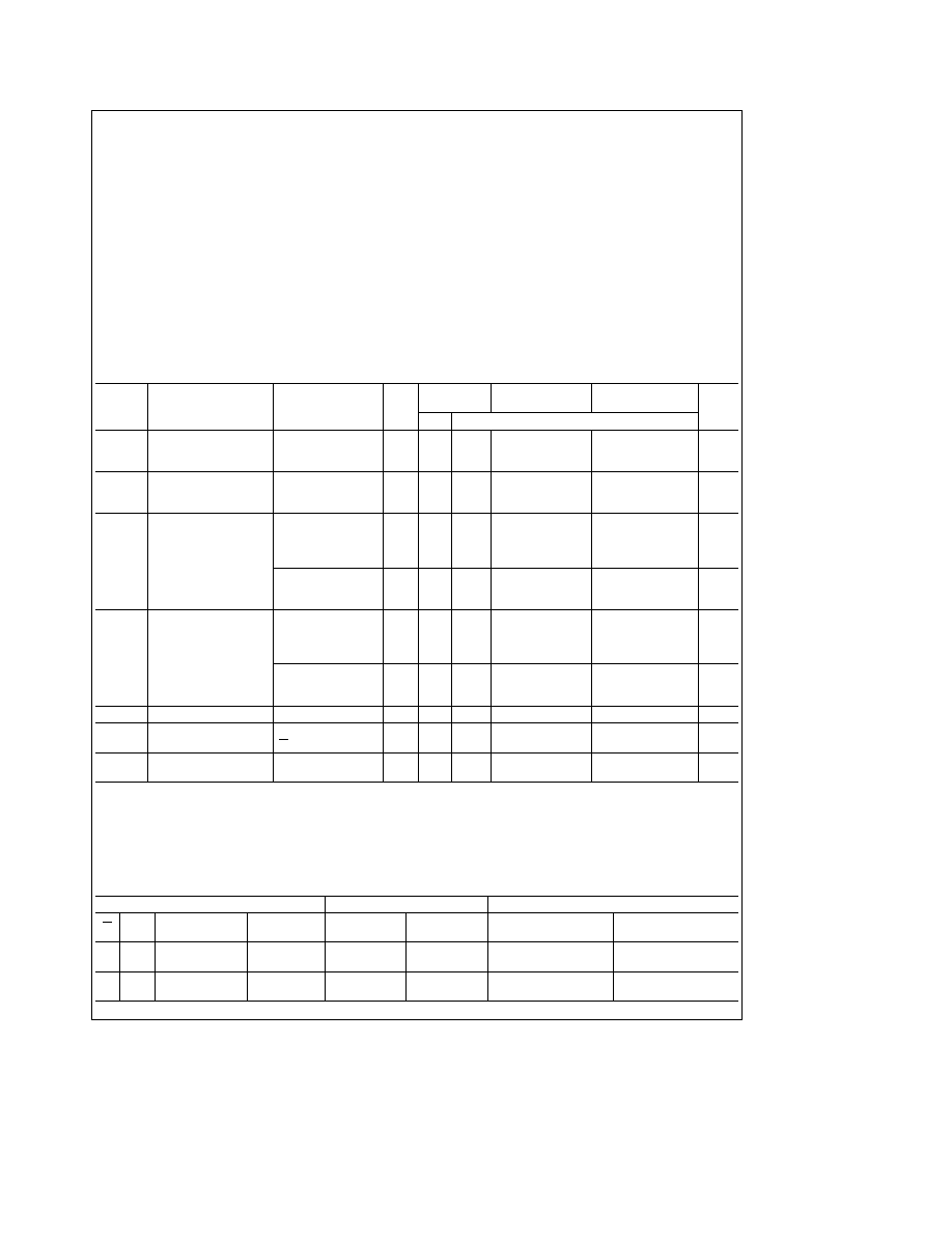
Truth Table
Inputs
Data I O
Operation or Function
G
DIR
CAB
CBA
SAB
SBA
A1 Thru A8
B1 Thru B8
'ALS646 'ALS647
'ALS648 'ALS649
'AS646
'AS648
X
X
u
X
X
X
Input
Not Specified
Store A B Unspecified
Store A B Unspecified
X
X
X
u
X
X
Not Specified
Input
Store B A Unspecified
Store B A Unspecified
H
X
u
u
X
X
Input
Input
Store A and B Data
Store A and B Data
H
X
H or L
H or L
X
X
Isolation hold storage
Isolation hold storage
2
Truth Table
(Continued)
Inputs
Data I O
Operation or Function
G
DIR
CAB
CBA
SAB
SBA
A1 Thru A8
B1 Thru B8
'ALS646 'ALS647
'ALS648 'ALS649
'AS646
'AS648
L
L
X
X
X
L
Output
Input
Real-Time B Data to A Bus
Real-Time B Data to A Bus
L
L
X
X
X
H
Stored B Data to A Bus
Stored B Data to A Bus
L
H
X
X
L
X
Input
Output
Real-Time A Data to B Bus
Real-Time A Data to B Bus
L
H
X
X
H
X
Stored A Data to B Bus
Stored A Data to B Bus
H
e
High Level L
e
Low Level X
e
Irrelevant
u
e
low-to-high level transition
The data output functions i e data at the bus pins may be enabled or disabled by various signals at the G and DIR inputs Data input functions are always enabled
The data output functions i e data at the bus pins will be stored on every low-to-high transition on the clock inputs
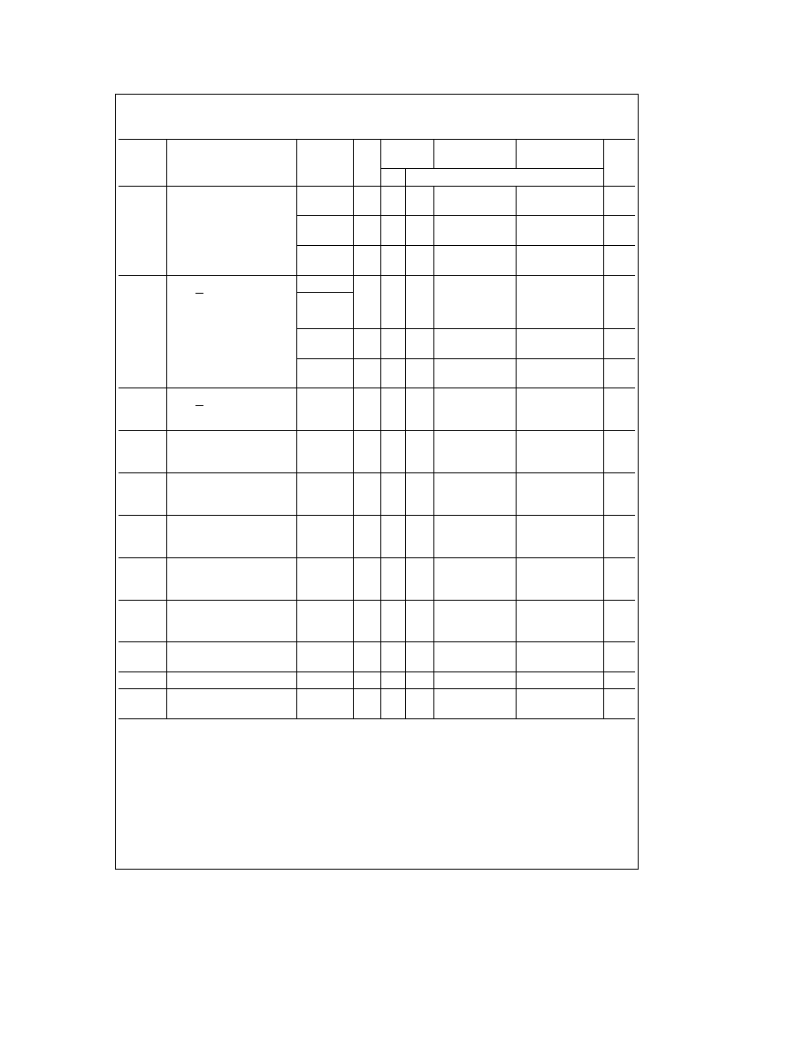
AC Electrical Characteristics
MM54HC646 MM74HC646 MM54HC648 MM74HC648
V
CC
e
5V T
A
e
25 C t
r
e
t
f
e
6 ns
Symbol
Parameter
Conditions
Typ
Guaranteed
Units
Limit
f
MAX
Maximum Operating
MHz
Frequency
t
PHL
t
PLH
Maximum Propagation
C
L
e
pF
ns
Delay A or B Input
to B or A Output
t
PHL
t
PLH
Maximum Propagation
C
L
e
pF
ns
Delay CBA or CAB
Input to A or B Output
t
PHL
t
PLH
Maximum Propagation
C
L
e
pF
ns
Delay SBA or SAB Input to A
or B Output with A or B high
t
PHL
t
PLH
Maximum Propagation
C
L
e
pF
ns
Delay SBA or SAB Input to A
or B Output with A or B low
t
PZH
t
PZL
Maximum Enable
R
L
e
kX
ns
Time G or DIR Input to
C
L
e
pF
A or B Output
t
PHZ
t
PLZ
Maximum Disable
R
L
e
kX
ns
Time G or DIR Input to
C
L
e
pF
A or B Output
AC Electrical Characteristics
MM54HC646 MM74HC646 MM54HC648 MM74HC648
V
CC
e
2 0 ≠ 6 0V C
L
e
50 pF t
r
e
t
f
e
6 ns (unless otherwise specified)
T
A
e
25 C
74HC
54HC
Symbol
Parameter
Conditions
V
CC
T
A
e b
40 to 85 C
T
A
e b
55 to 125 C
Units
Typ
Guaranteed Limits
f
MAX
Maximum Operating
C
L
e
pF
V
MHz
Frequency
V
MHz
V
MHz
t
PHL
t
PLH
Maximum Propagation
C
L
e
pF
V
ns
Delay A or B Input
C
L
e
pF
V
ns
to B or A Output
C
L
e
pF
V
ns
C
L
e
pF
V
ns
C
L
e
pF
V
ns
C
L
e
pF
V
ns
t
PHL
t
PLH
Maximum Propagation
C
L
e
pF
V
ns
Delay CBA or CAB
C
L
e
pF
V
ns
Input to A or B Output
C
L
e
pF
V
ns
C
L
e
pF
V
ns
C
L
e
pF
V
ns
C
L
e
pF
V
ns
3
AC Electrical Characteristics
MM54HC646 MM74HC646 MM54HC648 MM74HC648 (Continued)
V
CC
e
2 0
b
6 0V C
L
e
50 pF t
r
e
t
f
e
6 ns (unless otherwise specified)
T
A
e
25 C
74HC
54HC
Symbol
Parameter
Conditions
V
CC
T
A
e b
40 to 85 C T
A
e b
55 to 125 C Units
Typ
Guaranteed Limits
t
PHL
t
PLH
Maximum Propagation
C
L
e
50 pF
2 0V
85
170
214
253
ns
Delay SBA or SAB
C
L
e
150 pF 2 0V 110
220
277
328
ns
Input to A or B Output
C
L
e
50 pF
4 5V
17
34
43
51
ns
C
L
e
150 pF 4 5V
22
44
55
66
ns
C
L
e
50 pF
6 0V
14
29
36
43
ns
C
L
e
150 pF 6 0V
19
37
47
56
ns
t
PZL
t
PZL
Maximum Output Enable
R
L
e
1 kX
Time G Input or DIR to A or B
C
L
e
50 pF
2 0V
80
175
219
263
ns
Output
C
L
e
150 pF 2 0V 120
225
281
338
ns
C
L
e
50 pF
4 5V
23
35
44
53
ns
C
L
e
150 pF 4 5V
31
45
56
68
ns
C
L
e
50 pF
6 0V
21
30
37
45
ns
C
L
e
150 pF 6 0V
27
38
48
57
ns
t
PHZ
t
PLZ
Maximum Output Disable
R
L
e
1 kX
2 0V
85
175
219
263
ns
Time G Input to A or B
C
L
e
50 pF
4 5V
23
35
44
53
ns
Output
6 0V
21
30
37
45
ns
t
THL
t
TLH
Maximum Output Rise
2 0V
60
75
90
ns
and Fall Time
C
L
e
50 pF
4 5V
12
15
18
ns
6 0V
10
13
15
ns
t
S
Minimum Set Up Time
2 0V
100
125
150
ns
4 5V
20
25
30
ns
6 0V
17
21
25
ns
t
H
Minimum Hold Time
2 0V
0
0
0
ns
4 5V
0
0
0
ns
6 0V
0
0
0
ns
t
W
Minimum Pulse Width
2 0V
80
100
120
ns
of Clock
4 5V
16
20
24
ns
6 0V
14
18
21
ns
t
r
t
f
Maximum Input Rise and
2 0V
1000
1000
1000
ns
Fall Time
4 5V
500
500
500
ns
6 0V
400
400
400
ns
C
PD
Power Dissipation
90
pF
Capacitance (Note 5)
C
IN
Maximum Input Capacitance
5
10
10
10
pF
C
OUT
Maximum Output
15
20
20
20
pF
Capacitance
Note 5
C
PD
determines the no load dynamic power consumption P
D
e
C
PD
V
CC
2
f
a
I
CC
and the no load dynamic current consumption I
S
e
C
PD
V
CC
f
a
I
CC
Note 6
Refer to back of this section for Typical MM54 74HC AC Switching Waveforms and Test Circuits
4
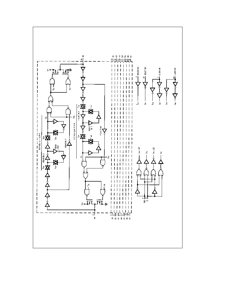
Logic Diagram
TLF5345
≠
3
5